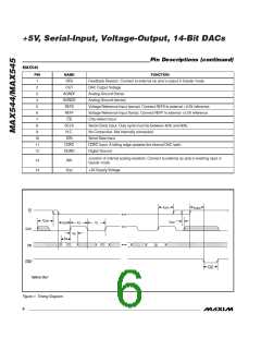
+5V, Serial-Input, Voltage-Output, 14-Bit DACs
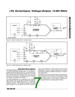
+5V
+2.5V
10µF
0.1µF
0.1µF
MC68XXXX
V
REF (REFF) (REFS)
DD
UNIPOLAR
OUT
PCS0
MOSI
SCLK
CS
MAX495
EXTERNAL OP AMP
OUT
DIN
MAX544/MAX545
SCLK
(GND)
(LDAC)
DGND
AGND_
(
) ARE FOR MAX545 ONLY
Figure 2a. Typical Operating Circuit—Unipolar Output
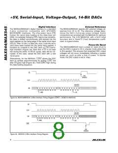
+5V
+2.5V
10µF
0.1µF
0.1µF
+5V
RFB
MC68XXXX
V
REFS
REFF
DD
R
INV
PCS0
MOSI
SCLK
IC1
CS
R
INV
FB
BIPOLAR
OUT
EXTERNAL OP AMP
MAX400
DIN
OUT
SCLK
LDAC
DGND
MAX545
-5V
(GND)
AGNDF
AGNDS
Figure 2b. Typical Operating Circuit—Bipolar Output
major-carry transitions. ꢁt also lowers the DAC output
impedance by a factor of eight compared to a standard
R-ꢂR ladder, allowing unbuffered operation in medium-
load applications.
Detailed Description
The MAX544/MAX545 voltage-output, 14-bit digital-to-
analog converters (DACs) offer full 14-bit performance
with less than ±.5ꢀLS integral linearity error and less
than ±.0ꢀLS differential linearity error, thus ensuring
monotonic performance. Lerial-data transfer minimizes
the number of package pins required.
The MAX545 provides matched bipolar offset resistors,
which connect to an external op amp for bipolar output
swings (Figure ꢂb). For optimum performance, the
MAX545 also provides a set of Kelvin connections to
the voltage-reference and analog-ground inputs.
The MAX544/MAX545 are composed of two matched
DAC sections, with an inverted R-ꢂR DAC forming the
ꢀLSs and the four MLSs derived from 15 identically
matched resistors. This architecture allows the lowest
glitch energy to be transferred to the DAC output on
_______________________________________________________________________________________
7

 MAXIM [ MAXIM INTEGRATED PRODUCTS ]