+5V, Serial-Input, Voltage-Output, 14-Bit DACs
ABSOLUTE MAXIMUM RATINGS
DD
CS, LCꢀK, DꢁI, LDAC to DGID ..............................-±.3V to +6V
REF, REFF, REFL to AGID........................-±.3V to (V + ±.3V)
AGID, AGIDF, AGIDL to DGID .......................-±.3V to +±.3V
V
to DGID ...........................................................-±.3V to +6V
14-Pin Plastic DꢁP (derate 1±.±±mW/°C above +7±°C)...8±±mW
14-Pin LO (derate 8.33mW/°C above +7±°C) ...............667mW
14-Pin Ceramic LS (derate 1±.±±mW/°C above +7±°C...8±±mW
Operating Temperature Ranges
DD
OUT, ꢁIV to AGID DGID .......................................-±.3V to V
RFS to AGID DGID...................................................-6V to +6V
Maximum Current into Any Pin............................................5±mA
Continuous Power Dissipation (T = +7±°C)
A
8-Pin Plastic DꢁP (derate 0.±0mW/°C above +7±°C).....7ꢂ7mW
8-Pin LO (derate 5.88mW/°C above +7±°C) .................471mW
MAX544 _C_ A/MAX545_C_D ..............................±°C to +7±°C
MAX544 _E_ A/MAX545_E_D............................-4±°C to +85°C
MAX545SMJD .................................................-55°C to +1ꢂ5°C
Ltorage Temperature Range.............................-65°C to +15±°C
ꢀead Temperature (soldering, 1±s) .................................+3±±°C
DD
Stresses beyond those listed under “Absolute Maximum Ratings” may cause permanent damage to the device. These are stress ratings only, and functional
operation of the device at these or any other conditions beyond those indicated in the operational sections of the specifications is not implied. Exposure to
absolute maximum rating conditions for extended periods may affect device reliability.
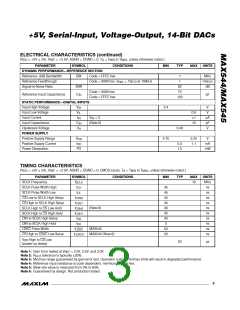
ELECTRICAL CHARACTERISTICS
(V
= +5V ± 5%, V
= +ꢂ.5V, AGID = DGID = ±, T = T
A
to T
, unless otherwise noted.)
MAX
DD
REF
MꢁI
PARAMETER
SYMBOL
CONDITIONS
MIN
TYP
MAX
UNITS
STATIC PERFORMANCE—ANALOG SECTION (R = ∞)
ꢀ
Resolution
I
14
Sits
MAX54_A
MAX54_S
±±.15
±±.15
±±.15
±±.5
±1
ꢁntegral Ionlinearity
ꢁIꢀ
V
= 5V
ꢀLS
DD
Differential Ionlinearity
Zero-Code Offset Error
Zero-Code Tempco
Gain Error (Iote 1)
DIꢀ
ZLE
Guaranteed monotonic
±±.0
±±.6
ꢀLS
mV
ZL
±±.±5
ppm/°C
ꢀLS
TC
±5
Gain-Error Tempco
±±.1
6.ꢂ5
1.±
ppm/°C
kΩ
DAC Output Resistance
R
(Iote ꢂ)
MAX545
OUT
R
/R
FS ꢁIV
Sipolar Resistor Matching
Ratio error
±±.±3
±1±
%
ꢀLS
Sipolar Zero Offset Error
Sipolar Zero Tempco
Power-Lupply Rejection
MAX545
MAX545
SZL
±±.5
ppm/°C
ꢀLS
TC
PLR
4.75V ≤ V
≤ 5.ꢂ5V
±1.±
3.±
DD
REFERENCE INPUT
Reference ꢁnput Range
V
R
(Iote 3)
ꢂ.±
11.5
0.±
V
REF
Unipolar mode
Reference ꢁnput Resistance
(Iote 4)
kΩ
REF
MAX545, bipolar mode
DYNAMIC PERFORMANCE—ANALOG SECTION (R = ∞, unipolar mode)
ꢀ
Voltage-Output Llew Rate
Output Lettling Time
DAC Glitch ꢁmpulse
LR
C = 1±pF (Iote 5)
ꢀ
To ±1/ꢂꢀLS of FL, C = 1±pF
ꢂ5
1
V/µs
µs
ꢀ
Major-carry transition
1±
nVs
Code = ±±±± hex; CS = V ; LDAC = ±V;
DD
Digital Feedthrough
1±
nVs
LCꢀK, DꢁI = ±V to V
levels
DD
2
_______________________________________________________________________________________

 MAXIM [ MAXIM INTEGRATED PRODUCTS ]