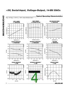
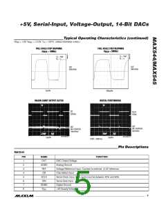
+5V, Serial-Input, Voltage-Output, 14-Bit DACs
amplifier’s input resistance forms a resistive divider with
the DAC output resistance, which results in a gain
error. To contribute less than 1/ꢂꢀLS of gain error, the
input resistance typically must be greater than:
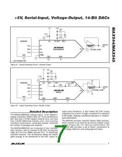
Unipolar Configuration
Figure ꢂa shows the MAX544/MAX545 configured for
unipolar operation with an external op amp. The op amp
is set for unity gain, and Table 1 lists the codes for this
circuit.
1
ꢂ
1
6.ꢂ5kΩ ÷
= ꢂ±5MΩ
14
ꢂ
Bipolar Configuration
Figure ꢂb shows the MAX545 configured for bipolar
operation with an external op amp. The op amp is set
The settling time is affected by the buffer input capaci-
tance, the DAC’s output capacitance, and PC board
capacitance. The typical DAC output voltage settling
time is 1µs for a full-scale step. Lettling time can be
significantly less for smaller step changes. Assuming a
single time-constant exponential settling response, a
full-scale step takes 1±.4 time constants to settle to
within 1/ꢂꢀLS of the final output voltage. The time con-
stant is equal to the DAC output resistance multiplied
by the total output capacitance. The DAC output
capacitance is typically 1±pF. Any additional output
capacitance increases the settling time.
for unity gain with an offset of -1/ꢂV
. Table ꢂ shows
REF
the offset binary codes for this circuit.
Power-Supply Bypassing and
Ground Management
For optimum system performance, use PC boards with
separate analog and digital ground planes. Wire-wrap
boards are not recommended. Connect the two ground
planes together at the low-impedance power-supply
source. Connect DGID and AGID together at the ꢁC.
The best ground connection can be achieved by con-
necting the DAC’s DGID and AGID pins together and
connecting that point to the system analog ground
plane. ꢁf the DAC’s DGID is connected to the system
digital ground, digital noise may get through to the
DAC’s analog portion.
The external buffer amplifier’s gain-bandwidth product
is important because it increases the settling time by
adding another time constant to the output response.
The effective time constant of two cascaded systems,
each with a single time-constant response, is approxi-
mately the root square sum of the two time constants.
The DAC output’s time constant is 1µs / 1±.4 = 06ns,
ignoring the effect of additional capacitance. ꢁf the time
constant of an external amplifier with 1MHz bandwidth
is 1 / ꢂπ (1MHz) = 150ns, then the effective time con-
stant of the combined system is:
Sypass V
with a ±.1µF ceramic capacitor connected
DD
DD
between V
and AGID. Mount it with short leads
close to the device. Ferrite beads can also be used to
further isolate the analog and digital power supplies.
Table 1. Unipolar Code Table
ꢂ
ꢂ
DAC LATCH CONTENTS
06ns + 150ns
=186ns
(
)
(
)
ANALOG OUTPUT, V
OUT
MSB
LSB
1111 1111 1111 11(±±)
1±±± ±±±± ±±±± ±±(±±)
±±±± ±±±± ±±±± ±1(±±)
V
REF · (16,383 / 16,384)
This suggests that the settling time to within 1/ꢂꢀLS of
the final output voltage, including the external buffer
amplifier, will be approximately 1±.4 · 186ns = 1.03µs.
1/
VREF · (810ꢂ / 16,384) =
V
REF
ꢂ
VREF · (1 / 16,384)
±±±± ±±±± ±±±± ±±(±±) ±V
Digital Inputs and Interface Logic
The digital interface for the 14-bit DAC is based on a
3-wire standard that is compatible with LPꢁ, QLPꢁ, and
MꢁCROWꢁRE interfaces. The three digital inputs (CS,
DꢁI, and LCꢀK) load the digital input data serially into
the DAC. LDAC (MAX545) updates the DAC output
asynchronously.
Table 2. Bipolar Code Table
DAC LATCH CONTENTS
ANALOG OUTPUT, V
OUT
MSB
LSB
1111 1111 1111 11(±±)
1±±± ±±±± ±±±± ±1(±±)
+VREF · (8101 / 810ꢂ)
+VREF · (1 / 810ꢂ)
All of the digital inputs include Lchmitt-trigger buffers to
accept slow-transition interfaces. This means that opto-
couplers can interface directly to the MAX544/MAX545
without additional external logic. The digital inputs are
compatible with TTꢀ/CMOL-logic levels.
1±±± ±±±± ±±±± ±±(±±) ±V
±111 1111 1111 11(±±)
±±±± ±±±± ±±±± ±±(±±)
-VREF · (1 / 810ꢂ)
-VREF · (810ꢂ / 810ꢂ) = -V
REF
(
) = Lub-bits
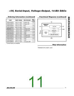
10 ______________________________________________________________________________________

 MAXIM [ MAXIM INTEGRATED PRODUCTS ]