2 -Wire S e ria l 8 -Bit DACs w it h
Ra il-t o -Ra il Ou t p u t s
78/MAX519
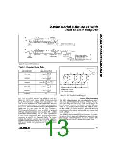
Furthermore if the transmission’s last command byte
following output byte is ignored. Subsequent pairs of
c omma nd /outp ut b yte s ove rwrite the inp ut la tc he s
(Figure 11b).
has PD high, the output latches are updated, but volt-
age outputs will not reflect the newly entered data
because the DAC enters power-down mode when the
STOP condition is detected. When in power-down, the
DAC outputs float. In this mode, the supply current is a
maximum of 20µA. A command byte with the PD bit low
returns the MAX517/MAX518/MAX519 to normal opera-
tion following a STOP condition, with the voltage out-
puts reflecting the output-latch contents (Figures 10a
and 10b). Because each subsequent command byte
overwrites the previous PD bit, only the last command
byte of a transmission affects the power-down state.
All c ha ng e s ma d e d uring a tra nsmission a ffe c t the
MAX517/MAX518/MAX519’s outp uts only whe n the
transmission ends and a STOP has been recognized.
The R0, R1, and R2 bits are reserved and must be set
to zero.
2
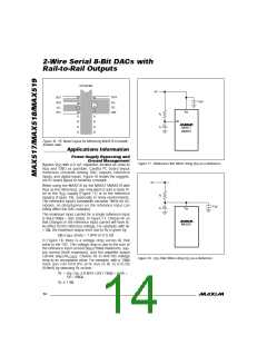
I C Co m p a t ib ilit y
The MAX517/MAX518/MAX519 are fully compatible
with e xis ting I2C s ys te ms . SCL a nd SDA a re hig h-
impedance inputs; SDA has an open drain that pulls
the data line low during the 9th clock pulse. Figure 12
shows a typical I2C application.
Setting the RST bit high clears the DAC input latches.
The DAC outputs remain unchanged until a STOP con-
dition is detected (Figure 11a). If a reset is issued, the
1
or
1
or
(PD)
0
(a)
SDA
0
1
0
AD2 AD1AD0 0
0
0
0
0
0
0
AD3
X
X
X
0
ADDRESS BYTE
ACK
COMMAND BYTE
ACK
STOP
START
CONDITION
DEVICE RETURNS TO
CONDITION NORMAL OPERATION
(
)
1
1
(b)
SDA
or or
(PD)
0
0
1
0
AD1AD0 0
0
0
0
0
0
0
0
0
0
0
0
0
0
0
0
AD3 AD2
X
X
ACK
ADDRESS BYTE
ACK
COMMAND BYTE
(ADDRESSING DAC0)
OUTPUT BYTE
(SET TO 0)
ACK
STOP
CONDITION
START
CONDITION
DAC0 INPUT
LATCH SET TO 0.
(
)
NOTE: X = DON'T CARE
DEVICE RETURNS TO NORMAL OPERATION.
(
)
DAC0 SET TO 0.
Figure 10. Returning to Normal Operation from Power-Down
1
1
or or
AD3 AD2
(a)
SDA
(RST)
1
0
1
0
AD1AD0 0
0
0
0
0
0
0
X
X X
ADDRESS BYTE
ACK
COMMAND BYTE
ACK
STOP
CONDITION
START
CONDITION
ALL INPUT LATCHES
(
)
SET TO 0.
ALL OUTPUTS
SET TO 0.
1
1
(
)
(b)
SDA
or or
(RST)
1
0
1
0
AD1AD0 0
0
0
0
0
0
0
0
AD3 AD2
X
X
X
X X X X X X X X
ACK ADDITIONAL
COMMAND BYTE/
OUTPUT BYTE PAIRS
"DUMMY"
OUTPUT BYTE
ADDRESS BYTE
ACK
COMMAND BYTE
ACK
STOP
CONDITION
START
CONDITION
ALL INPUT LATCHES
SET TO 0.
DAC OUTPUTS SET TO 0 UNLESS
CHANGED BY ADDITIONAL COMMAND
BYTE/OUTPUT BYTE PAIRS.
(
)
NOTE: X = DON'T CARE
(
)
Figure 11. Resetting DAC Outputs
______________________________________________________________________________________ 11

 MAXIM [ MAXIM INTEGRATED PRODUCTS ]