2 -Wire S e ria l 8 -Bit DACs w it h
Ra il-t o -Ra il Ou t p u t s
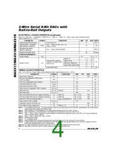
SDA
t
BUF
t
,
t ,
SU STA
SU DAT
t
,
HD STA
t
,
SU STO
t
t ,
HD DAT
LOW
SCL
t
HIGH
t
,
HD STA
t
R
t
F
START CONDITION
REPEATED START CONDITION
STOP CONDITION START CONDITION
Figure 2. Two-Wire Serial Interface Timing Diagram
The address byte and pairs of command and output
bytes are transmitted between the START and STOP con-
ditions. The SDA state is allowed to change only while
SCL is low, with the exception of START and STOP condi-
tions. SDA’s state is sampled, and therefore must remain
stable while SCL is high. Data is transmitted in 8-bit
bytes. Nine clock cycles are required to transfer the data
bits to the MAX517/MAX518/MAX519. Set SDA low dur-
ing the 9th clock cycle as the MAX517/MAX518/MAX519
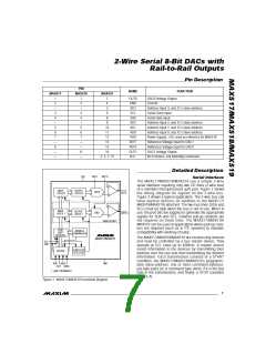
+1V
+4V
REF0
REF1
µC
DUAL
DAC
SDA
SCL
78/MAX519
R
C
1k
MAX519
SCL
SDA
AD0
AD1
AD2
AD3
OFFSET ADJUSTMENT
GAIN ADJUSTMENT
OUT0
OUT1
pull SDA low during this time. R (see Figure 3) limits the
C
current that flows during this time if SDA stays high for
short periods of time.
The START and STOP Conditions
When the bus is not in use, both SCL and SDA must be
high. A bus master signals the beginning of a transmis-
sion with a START condition by transitioning SDA from
high to low while SCL is high (Figure 5). When the mas-
ter has finished communicating with the slave, it issues
a STOP condition by transitioning SDA from low to high
while SCL is high. The bus is then free for another
transmission.
DUAL
DAC
MAX518
SCL
SDA
AD0
AD1
BRIGHTNESS ADJUSTMENT
CONTRAST ADJUSTMENT
OUT0
OUT1
The Slave Address
The MAX517/MAX518/MAX519 each have a 7-bit long
slave address (Figure 6). The first three bits (MSBs) of
the slave address have been factory programmed and
are always 010. In addition, the MAX517 and MAX518
have the next two bits factory programmed to 1s. The
logic state of the address inputs (AD0 and AD1 on the
MAX517/MAX518; AD0, AD1, AD2, and AD3 on the
MAX519) de te rmine the LSB b its of the 7-bit sla ve
address. These input pins may be connected to VDD or
DGND, or they may be actively driven by TTL or CMOS
logic levels. The MAX517/MAX518 have four possible
slave addresses and therefore a maximum of four of
+2.5V
REF0
OUT0
SINGLE
DAC
MAX517
SCL
SDA
AD0
AD1
THRESHOLD ADJUSTMENT
+5V
Figure 3. MAX517/MAX518/MAX519 Application Circuit
_______________________________________________________________________________________
8

 MAXIM [ MAXIM INTEGRATED PRODUCTS ]