2 -Wire S e ria l 8 -Bit DACs w it h
Ra il-t o -Ra il Ou t p u t s
78/MAX519
______________________________________________________________P in De s c rip t io n
PIN
NAME
FUNCTION
MAX517
MAX518
MAX519
1
2
1
2
1
OUT0
GND
AD3
DAC0 Voltage Output
Ground
4
—
3
—
3
5
Address Input 3; sets IC’s slave address
Serial Clock Input
6
SCL
SDA
AD2
4
4
8
Serial Data Input
—
5
—
5
9
Address Input 2; sets IC’s slave address
Address Input 1; sets IC’s slave address
Address Input 0; sets IC’s slave address
Power Supply, +5V; used as reference for MAX518
Reference Voltage Input for DAC1
Reference Voltage Input for DAC0
DAC1 Voltage Output
10
AD1
6
6
11
AD0
7
7
12
13
VDD
REF1
REF0
OUT1
N.C.
—
8
—
—
8
15
—
—
16
—
2, 3, 7, 14
No Connect—not internally connected.
_______________De t a ile d De s c rip t io n
V
DD
REF0
(REF1)
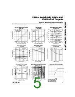
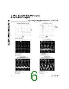
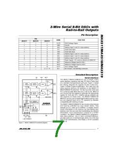
S e ria l In t e rfa c e
The MAX517/MAX518/MAX519 us e a s imp le 2-wire
serial interface requiring only two I/O lines (2-wire bus)
of a standard microprocessor (µP) port. Figure 2 shows
the timing d ia g ra m for s ig na ls on the 2-wire b us .
Figure 3 shows a typical application. The 2-wire bus can
ha ve s e ve ra l d e vic e s (in a d d ition to the MAX517/
MAX518/MAX519) attached. The two bus lines (SDA and
SCL) must be high when the bus is not in use. When in
use, the port bits are toggled to generate the appropriate
signals for SDA and SCL. External pull-up resistors are
not re q uire d on the s e line s . The MAX517/MAX518/
MAX519 can be used in applications where pull-up resis-
INPUT
OUTPUT
LATCH 0
DAC0
OUT0
LATCH 0
INPUT
LATCH 1
OUTPUT
LATCH 1
DAC1
(OUT1)
MAX519 ONLY
2
tors are required (such as in I C systems) to maintain
compatibility with existing circuitry.
8-BIT
SHIFT
REGISTER
ADDRESS
COMPARATOR
The MAX517/MAX518/MAX519 are receive-only devices
and must be controlled by a bus master device. They
operate at SCL rates up to 400kHz. A master device
sends information to the devices by transmitting their
address over the bus and then transmitting the desired
information. Each transmission consists of a START
condition, the MAX517/MAX518/MAX519’s programm-
able slave-address, one or more command-byte/out-
put-byte pairs (or a command byte alone, if it is the last
byte in the transmission), and finally, a STOP condition
(Figure 4).
MAX517/MAX519
SCL
SDA
START/STOP
DETECTOR
DECODE
AD0 (AD2)
AD1 (AD3)
GND
( ) ARE FOR MAX519
Figure 1. MAX517/MAX519 Functional Diagram
_______________________________________________________________________________________
7

 MAXIM [ MAXIM INTEGRATED PRODUCTS ]