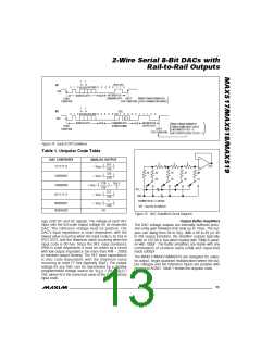
2 -Wire S e ria l 8 -Bit DACs w it h
Ra il-t o -Ra il Ou t p u t s
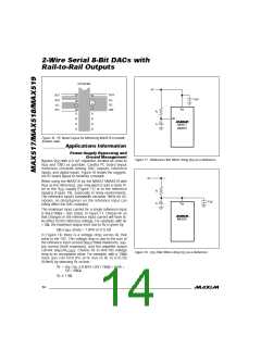
SYSTEM GND
+5V
OUT1
OUT0
0.1µF
REF0
N.C.
N.C.
N.C.
GND
V
DD
REF1
R
F
REF_
C
F
MAX517
MAX519
Figure 16. PC Board Layout for Minimizing MAX519 Crosstalk
(bottom view)
__________Ap p lic a t io n s In fo rm a t io n
P o w e r-S u p p ly Byp a s s in g a n d
Gro u n d Ma n a g e m e n t
Bypass V with a 0.1µF capacitor, located as close to
Figure 17. Reference Filter When Using V as a Reference
DD
DD
V
DD
and GND as possible. Careful PC board layout
minimizes crosstalk among DAC outputs, reference
inputs, and digital inputs. Figure 16 shows the suggest-
ed PC board layout to minimize crosstalk.
78/MAX519
+5V
When using the MAX518 (or the MAX517/MAX519 with
V
DD
as the reference), you may want to add a noise fil-
ter to the V
supply (Figure 17) or to the reference
DD
R
F
input(s) (Figure 18), especially in noisy environments.
The reference input’s bandwidth exceeds 1MHz for AC
signals, so disturbances on the reference input can
easily affect the DAC output(s).
0.1µF
C
F
V
DD
The maximum input current for a single reference input
is V /16kΩ = I
(max). In Figure 17, choose R so
REF
REF
F
that changes in the reference input current will have lit-
tle effect on the reference voltage. For example, with R
MAX518
F
= 6Ω, the maximum output error due to R is given by:
F
6Ω x I
(max) = 1.9mV or 0.1LSB
REF
In Figure 18, there is a voltage drop across R that
F
adds to the TUE. This voltage drop is due to the sum of
the reference input current (V /16kΩ maximum), sup-
REF
ply current (6mA maximum), and the amplifier output
current (V
/R
). Choose R to limit this voltage
REF LOAD F
Figure 18. V Filter When Using V as a Reference
DD
DD
drop to an acceptable value. For example, with a 10kΩ
loa d , you c a n limit the e rror d ue to R to 0.5LSB
F
(9.8mV) by selecting R so that:
F
R
= V / I ≤ 9.8mV / (5V / 16kΩ + 6mA +
R R
F F
5V / 10kΩ)
≤ 1.4Ω
F
F
R
14 ______________________________________________________________________________________

 MAXIM [ MAXIM INTEGRATED PRODUCTS ]