2 -Wire S e ria l 8 -Bit DACs w it h
Ra il-t o -Ra il Ou t p u t s
78/MAX519
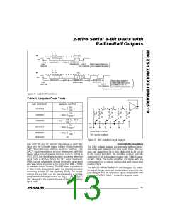
SLAVE ADDRESS BYTE
COMMAND BYTE
OUTPUT BYTE
SDA
SCL
MSB
LSB
ACK
MSB
LSB ACK
MSB
LSB
ACK
STOP CONDITION
START CONDITION
Figure 4. A Complete Serial Transmission
R2
R1
R0 RST
PD
A0/0 ACK
LSB
X
X
SDA
SDA
MSB
SCL
SCL
START CONDITION
STOP CONDITION
R2, R1, R0: RESERVED BITS. SET TO 0.
RST: RESET BIT, SET TO 1 TO RESET ALL DAC REGISTERS.
Figure 5. All communications begin with a START condition and
end with a STOP condition, both generated by a bus master.
PD: POWER-DOWN BIT. SET TO 1 TO PLACE THE DEVICE IN THE 4µA SHUTDOWN
MODE. SET TO 0 TO RETURN TO THE NORMAL OPERATIONAL STATE.
A0: ADDRESS BIT. DETERMINES WHICH DAC'S INPUT LATCH RECEIVES THE 8 BITS
OF DATA IN THE NEXT BYTE. SET TO 0 FOR MAX517.
SLAVE ADDRESS
ACK: ACKNOWLEDGE BIT. THE MAX517/MAX518/MAX519 PULLS SDA LOW DURING
THE 9TH CLOCK PULSE.
0
1
0
1 or
AD3 AD2
1 or AD1
AD0
0
ACK
X: DON’T CARE.
SDA
SCL
LSB
Figure 7. Command Byte
SLAVE ADDRESS BITS AD0, AD1, AD2, AND AD3 CORRESPOND TO THE LOGIC
STATE OF THE ADDRESS INPUT PINS.
Figure 6. Address Byte
these devices may share the bus. The MAX519 has 16
possible slave addresses. The eighth bit (LSB) in the
slave address byte should be low when writing to the
MAX517/MAX518/MAX519.
ignored. If an output byte follows the command byte,
A0 of the command byte indicates the digital address
of the DAC whose input data latch receives the digital
outp ut d a ta . Se t this b it to 0 whe n writing to the
MAX517. The data is transferred to the DAC’s output
latch during the STOP condition following the transmis-
sion. This allows both DACs of the MAX518/MAX519 to
be updated simultaneously (Figure 8).
The MAX517/MAX518/MAX519 monitor the bus continu-
ously, waiting for a START condition followed by their
slave address. When a device recognizes its slave
address, it is ready to accept data.
Se tting the PD b it hig h p owe rs d own the MAX517/
MAX518/MAX519 following a STOP condition (Figure
9a). If a command byte with PD set high is followed by
an output byte, the addressed DAC’s input latch will be
updated and the data will be transferred to the DAC’s
output latch following the STOP condition (Figure 9b).
The Command Byte and Output Byte
A command byte follows the slave address. Figure 7
shows the format for the command byte. A command
byte is usually followed by an output byte unless it is
the last byte in the transmission. If it is the last byte, all
b its e xc e p t PD (p owe r-d own) a nd RST (re s e t) a re
_______________________________________________________________________________________
9

 MAXIM [ MAXIM INTEGRATED PRODUCTS ]