MAX31865
RTD-to-Digital Converter
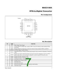
Pin Configuration
TOP VIEW
15
14
13
12
11
GND2
10
9
GND1 16
FORCE-
N.C. 17
MAX31865
8
DRDY 18
RTDIN-
RTDIN+
FORCE2
DVDD
7
19
20
6
V
DD
EP
+
1
2
3
4
5
TQFN
(5mm x 5mm)
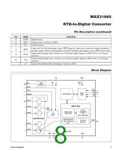
Pin Description
PꢀN
NAME
FUNCTꢀON
1
BIAS
Bias Voltage Output (V
)
BIAS
Positive Reference Voltage Input. Connect to BIAS. Connect the reference resistor between REFIN+
and REFIN-.
2
REFIN+
REFIN-
3
4
Negative Reference Voltage Input. Connect the reference resistor between REFIN+ and REFIN-.
ISENSOR Low Side of R
Connect to REFIN-.
REF.
High-Side RTD Drive. Connect to FORCE2 when using the 3-wire connection configuration. Protected to
Q50V.
5
6
FORCE+
FORCE2
Positive Input Used in 3-Wire Only. When in the 3-wire connection configuration, connect to FORCE+.
When in the 2-wire or 4-wire connection configuration, connect to ground. Protected to Q50V.
7
RTDIN+
RTDIN-
Positive RTD Input. Protected to Q50V.
Negative RTD Input. Protected to Q50V.
8
9
FORCE- Low-Side RTD Return. Protected to Q50V.
10
11
12
13
14
GND2
SDI
Analog Ground. Connect to GND1.
Serial-Data Input
SCLK
Serial-Data Clocꢀ Input
CS
Active-Low Chip Select. Set CS low to enable the serial interface.
SDO
Serial-Data Output
Maxim Integrated
7

 MAXIM [ MAXIM INTEGRATED PRODUCTS ]