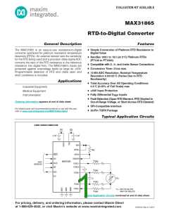
MAX31865
RTD-to-Digital Converter
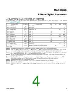
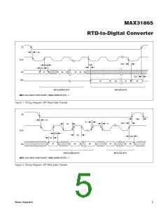
AC ELECTRꢀCAL CHARACTERꢀSTꢀCS: SPꢀ ꢀNTERFACE
(3.0V P V
P 3.6V, T = -40NC to +125NC, unless otherwise noted. Typical values are T = +25NC, V
= V
= 3.3V.) (Notes 3
DVDD
DD
A
A
DD
and 7) (Figure 1 and Figure 2)
PARAMETER
Data to SCLK Setup
SCLK to Data Hold
SCLK to Data Valid
SCLK Low Time
SYMBOL
CONDꢀTꢀONS
MꢀN
35
TYP
MAX
UNꢀTS
ns
t
(Notes 8, 9)
(Notes 8, 9)
(Notes 8, 9, 10)
(Note 9)
DC
t
t
35
ns
CDH
CDD
80
ns
t
100
100
DC
ns
CL
SCLK High Time
t
(Note 9)
ns
CH
SCLK Frequency
SCLK Rise and Fall
CS to SCLK Setup
SCLK to CS Hold
CS Inactive Time
t
(Note 9)
5.0
MHz
ns
CLK
t , t
R
(Note 9)
200
F
t
(Note 9)
400
100
400
ns
CC
t
(Note 9)
ns
CCH
t
(Note 9)
ns
CWH
t
(Notes 8, 9)
40
ns
CS to Output High-Z
CDZ
Address 01h or 02h Decoded to
DRDY High
t
After RTD register read access (Note 9)
50
ns
DRDYH
Note 2: All voltages are referenced to ground when common. Currents entering the IC are specified positive.
Note 3: Limits are 100% production tested at T = +25°C and/or T = +85°C. Limits over the operating temperature range and rel-
A
A
evant supply voltage range are guaranteed by design and characterization. Typical values are not guaranteed.
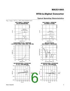
Note 4: For 15-bit settling, a wait of at least 10.5 time constants of the input RC networꢀ is required. Max startup time is calculated
with a 10ꢀω reference resistor and a 0.1µF capacitor across the RTD inputs.
Note 5: The first conversion after enabling continuous conversion mode taꢀes a time equal to the single conversion time for the
respective notch frequency.
Note 6: Specified with no load on the bias pin as the sum of analog and digital currents. No active communication. If the RTD
input voltage is greater than the input reference voltage, then an additional 400µA I
Note 7: All timing specifications are guaranteed by design.
can be expected.
DD
Note 8: Measured at V = 0.7V x V
Note 9: Measured with 50pF load.
or V = 0.3 x V and 10ms maximum rise and fall times.
IH
DVDD
IL
DVDD
Note 10: Measured at V
= 0.7 x V
or V = 0.3 x V
. Measured from the 50% point of SCLK to the V
minimum of
OH
DVDD
OL
DVDD
OH
SDO.
Maxim Integrated
4

 MAXIM [ MAXIM INTEGRATED PRODUCTS ]