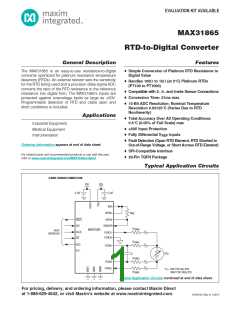
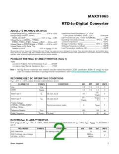
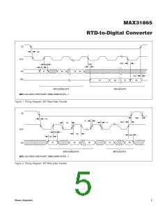
MAX31865
RTD-to-Digital Converter
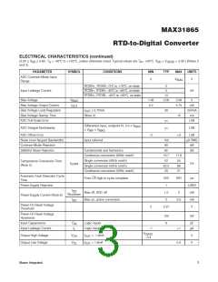
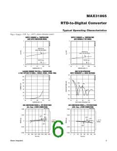
ELECTRꢀCAL CHARACTERꢀSTꢀCS (continued)
(3.0V P V
P 3.6V, T = -40NC to +125NC, unless otherwise noted. Typical values are T = +25NC, V
= V
= 3.3V.) (Notes 2
DVDD
DD
A
A
DD
and 3)
PARAMETER
SYMBOL
CONDꢀTꢀONS
MꢀN
TYP
MAX
UNꢀTS
ADC Common-Mode Input
Range
0
V
V
BIAS
RTDIN+, RTDIN-, 0NC to +70NC, on-state
RTDIN+, RTDIN-, -40NC to +85NC, on-state
2
Input Leaꢀage Current
5
nA
RTDIN+, RTDIN-, -40NC to 100NC, on-state
14
Bias Voltage
V
1.95
0.2
2.00
2.06
5.75
V
mA
BIAS
Bias Voltage Output Current
Bias Voltage Load Regulation
Bias Voltage Startup Time
ADC Full-Scale Error
I
OUT
I
P 5.75mA
30
mV/mA
ms
OUT
(Note 4)
10
LSB
±1
±1
Differential Input, endpoint fit, 0.3 x V
P V
BIAS
ADC Integral Nonlinearity
LSB
P V
REF
BIAS
ADC Offset Error
-3
+3
LSB
FV RMS
dB
Noise (over Nyquist Bandwidth)
Common-Mode Rejection
50/60Hz Noise Rejection
Input referred
150
90
Fundamental and harmonics
82
dB
Continuous conversion (60Hz notch)
Single conversion (60Hz notch)
Single conversion (50Hz notch)
Continuous conversion (50Hz notch)
16.7
52
17.6
55
Temperature Conversion Time
(Note 5)
t
ms
CONV
62.5
20
66
21
Automatic Fault Detection Cycle
Time
550
1
600
Fs
LSB/V
mA
mA
V
From CS high to cycle complete
Power-Supply Rejection
I
DD
Bias off, ADC off
1.5
2
3
Shutdown
Power-Supply Current (Note 6)
I
Bias on, active conversion
3.5
DD
Power-On Reset Voltage
Threshold
2
2.27
Power-On Reset Voltage
Hysteresis
120
6
mV
Input Capacitance
C
Logic inputs
Logic inputs
pF
IN
Input Leaꢀage Current
I
-1
+1
FA
L
V
- 0.4
DVDD
Output High Voltage
Output Low Voltage
V
I
I
= -1.6mA
= 1.6mA
V
V
OH
OUT
OUT
V
0.4
OL
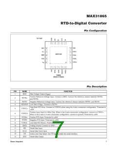
Maxim Integrated
3

 MAXIM [ MAXIM INTEGRATED PRODUCTS ]