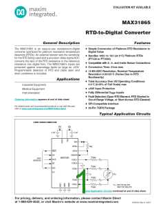
MAX31865
RTD-to-Digital Converter
ABSOLUTE MAXꢀMUM RATꢀNGS
Voltage Range on V
Relative to GND1............-0.3V to +4.0V
Continuous Power Dissipation (T = +70NC)
DD
A
Voltage Range on BIAS, REFIN+,
REFIN-, ISENSOR................................. -0.3V to (V
Voltage Range on FORCE+, FORCE2,
FORCE-, RTDIN+, RTDIN- Relative to GND1 ....-50V to +50V
Voltage Range on DVDD Relative to DGND........-0.3V to +4.0V
Voltage Range on All Digital Pins
TQFN (derate 34.5mW/NC above +70NC)...............2758.6mW
ESD Protection (all pins, Human Body Model)................... 2ꢀV
Operating Temperature Range........................ -40NC to +125NC
Junction Temperature .....................................................+150NC
Storage Temperature Range............................ -65NC to +150NC
Soldering Temperature (reflow) ......................................+260NC
Lead Temperature (soldering,10s) .................................+300NC
+ 0.3V)
DD
Relative to DGND ............................. -0.3V to (V
+ 0.3V)
DVDD
Stresses beyond those listed under “Absolute Maximum Ratings” may cause permanent damage to the device. These are stress ratings only, and functional opera-
tion of the device at these or any other conditions beyond those indicated in the operational sections of the specifications is not implied. Exposure to absolute
maximum rating conditions for extended periods may affect device reliability.
PACKAGE THERMAL CHARACTERꢀSTꢀCS (Note 1)
TQFN
Junction-to-Ambient Thermal Resistance (q ) ..........29°C/W
JA
Junction-to-Case Thermal Resistance (q ).................2°C/W
JC
Note 1: Pacꢀage thermal resistances were obtained using the method described in JEDEC specification JESD51-7, using a four-layer
board. For detailed information on pacꢀage thermal considerations, refer to www.maximintegrated.com/thermal-tutorial.
RECOMMENDED DC OPERATꢀNG CONDꢀTꢀONS
(T = -40NC to +125NC, unless otherwise noted.) (Notes 2 and 3)
A
PARAMETER
SYMBOL
CONDꢀTꢀONS
MꢀN
3.0
TYP
3.3
MAX
3.6
UNꢀTS
V
V
V
V
DD
DD
DVDD
V
3.0
3.3
3.6
DVDD
0.3 x
Input Logic 0
Input Logic 1
V
-0.3
V
V
CS, SDI, SCLK
CS, SDI, SCLK
IL
V
DVDD
0.7 x
V
DVDD
V
IH
V
+ 0.3
DVDD
Analog Voltages
(FORCE+,FORCE2, FORCE-,
RTDIN+, RTDIN-)
Normal conversion results
Per lead
0
V
V
BIAS
Reference Resistor
Cable Resistance
R
350
0
10ꢀ
50
I
I
REF
R
CABLE
ELECTRꢀCAL CHARACTERꢀSTꢀCS
(3.0V P V
P 3.6V, T = -40NC to +125NC, unless otherwise noted. Typical values are T = +25NC, V
= V
= 3.3V.) (Notes 2
DD
A
A
DD
DVDD
and 3)
PARAMETER
SYMBOL
CONDꢀTꢀONS
No missing codes
MꢀN
TYP
MAX
UNꢀTS
ADC Resolution
15
Bits
ADC Full-Scale Input Voltage
(RTDIN+ - RTDIN-)
REFIN+ -
REFIN-
V
Maxim Integrated
2

 MAXIM [ MAXIM INTEGRATED PRODUCTS ]