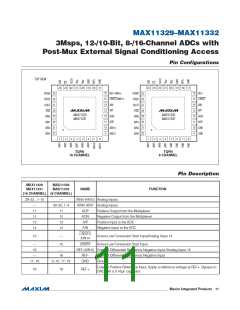
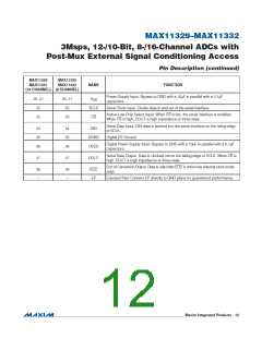
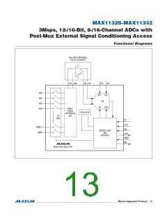
MAX11329–MAX11332
3Msps, 12-/10-Bit, 8-/16-Channel ADCs with
Post-Mux External Signal Conditioning Access
in single-ended or differential configuration. The external
buffering stage should be designed to properly drive the
input sampling network of the ADC.
mode to generate the serial clock signal. Select the SCLK
frequency of 48MHz or less, and set clock polarity (CPOL)
and phase (CPHA) in the control registers to the same
value. The MAX11329–MAX11332 operate with SCLK
idling high, and thus operate with CPOL = CPHA = 1.
The external buffer should also have very high input
impedance (low-leakage current) to ensure best linearity.
If additional signal processing is not required, connect
AOP to AIP and AON to AIN. It is recommended to limit
the source impedance to not affect the sampling accu-
racy of the ADC causing degradation in linearity and total
harmonic distortion. See the SINAD vs. Input Resistance
graph in the Typical Operating Characteristics.
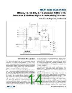
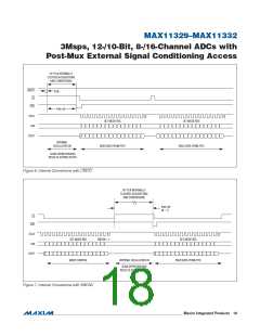
Set CS low to latch input data at DIN on the rising edge
of SCLK. Output data at DOUT is updated on the falling
edge of SCLK. A high-to-low transition on CS samples
the analog inputs and initiates a new frame. A frame is
defined as the time between two falling edges of CS.
There is a minimum of 16 bits per frame. The serial data
input, DIN, carries data into the control registers clocked
in by the rising edge of SCLK. The serial data output,
DOUT, delivers the conversion results and is clocked out
by the falling edge of SCLK. DOUT is a 16-bit data word
containing a 4-bit channel address, followed by a 12-bit
conversion result led by the MSB when CHAN_ID is set
to 1 in the ADC Mode Control register (Figure 2a). When
CHAN_ID is set to 1 keep the SCLK high for at least 25ns
before the CS falling edge (Figure 2b). When CHAN_ID is
set to 0 (external clock mode only), the 16-bit data word
includes a leading zero and the 12-bit conversion result
is followed by 3 trailing zeros (Figure 2c). In the 10-bit
conversion result is followed by 5 trailing zeros.
Input Bandwidth
The ADC’s input-tracking circuitry features a 500MHz
small-signal full-linear bandwidth to digitize high-speed
transient events and measure periodic signals with
bandwidths exceeding the ADC’s sampling rate by using
undersampling techniques. Anti-alias filtering of the input
signals is necessary to avoid high-frequency signals
aliasing into the frequency band of interest.
3-Wire Serial Interface
The MAX11329–MAX11332 feature a serial interface
compatible with SPI/QSPI and MICROWIRE devices. For
SPI/QSPI, ensure the CPU serial interface runs in master
CS
1
2
3
4
5
6
7
8
9
10
11
12
13
14
15
16
SCLK
DIN
DI[15] DI[14]
DI[1] DI[0]
DOUT
Ch[3] Ch[2] Ch[1] Ch[0] MSB MSB-1
LSB+1 LSB
Figure 2a. External Clock Mode Timing Diagram with CHAN_ID=1
CS
1
2
3
4
5
6
7
8
9
10
11
12
13
14
15
16
SCLK
DIN
t
> t
QUIET SCLK
DI[15]
DI[1] DI[0]
DOUT
Ch[3] Ch[2] Ch[1] Ch[0] MSB MSB-1
LSB+1 LSB
Figure 2b. External Clock Mode Timing Diagram with CHAN_ID=1 for Best Performance
���������������������������������������������������������������� Maxim Integrated Products 15

 MAXIM [ MAXIM INTEGRATED PRODUCTS ]