MAX11329–MAX11332
3Msps, 12-/10-Bit, 8-/16-Channel ADCs with
Post-Mux External Signal Conditioning Access
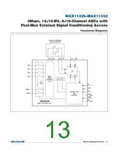
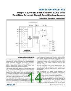
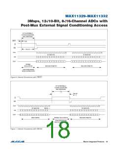
Functional Diagrams (continued)
AOP AON
AIN AIP
REF+ REF-
AIN0
AIN1
AIN2
AIN3
REF+
ADC
REF-
CS
SCLK
SINGLE-
ENDED/
OSCILLATOR
DIFFERENTIAL
BUS
I/P
MUX
CS
SCLK
DIN
AIN(N-1)
AIN(N)
CONTROL LOGIC
AND
SEQUENCER
DOUT
CNVST
EOC
MAX11329–MAX11332
is also supported in this mode improving SNR for noisy
input signals. All input channels are configurable for sin-
gle-ended, fully differential or pseudo-differential inputs
in unipolar or bipolar mode. The MAX11329–MAX11332
operate from a 2.35V to 3.6V supply and consume only
15.2mW at 3Msps.
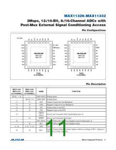
Detailed Description
The MAX11329–MAX11332 are 12-/10-bit with external
reference and industry-leading 500kHz, full linear band-
width, high-speed, low-power, serial output successive
approximation register (SAR) analog-to-digital converters
(ADC). These devices feature scan mode, internal aver-
aging to increase SNR, and AutoShutdown.
The MAX11329–MAX11332 include AutoShutdown, fast
wake-up, and a high-speed 3-wire serial interface. The
devices feature full power-down mode for optimal power
management.
The external clock mode features the SampleSet technol-
ogy, a user-programmable analog input channel sequenc-
er. The user may define and load a unique sequencing
pattern into the ADC allowing both high- and low-frequen-
cy inputs to be converted without interface activity. This
feature frees the controlling unit for other tasks while lower-
ing overall system noise and power consumption.
Data is converted from analog voltage sources in a
variety of channel and data-acquisition configurations.
Microprocessor (FP) control is made easy through a 3-wire
SPI-/QSPI-/MICROWIRE-compatible serial interface.
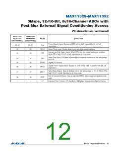
AOP and AON are the output pins of the internal multi-
plexer while AIP and AIN are the ADC inputs which are all
accessible externally through pins. This allows flexibility
to the system designer to process all signals through one
PGA (programmable gain amplifier), filter or gain stage
The MAX11329–MAX11332 include internal clock. The
internal clock mode features an integrated FIFO, allowing
data to be sampled at high speed and then held for read-
out at any time or at a lower clock rate. Internal averaging
���������������������������������������������������������������� Maxim Integrated Products 14

 MAXIM [ MAXIM INTEGRATED PRODUCTS ]