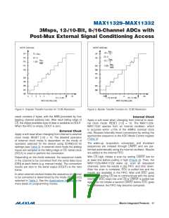
MAX11329–MAX11332
3Msps, 12-/10-Bit, 8-/16-Channel ADCs with
Post-Mux External Signal Conditioning Access
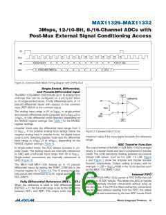
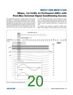
OUTPUT CODE (hex)
OUTPUT CODE (hex)
V
REF+
+FS =
7FF
FFF
FFE
FFD
FFC
FFB
FS = V
ZS = 0
1 LSB =
REF+
2
ZS = 0
7FE
-V
REF+
V
REF+
-FS =
2
V
4096
REF+
1 LSB =
001
000
FFF
FFE
4096
004
003
002
001
000
801
800
0
1
2
3
4
FS
-FS
0
+FS
FS -1.5 LSB
INPUT VOLTAGE (LSB)
-FS +0.5 LSB
+FS -1.5 LSB
INPUT VOLTAGE (LSB)
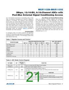
Figure 4. Unipolar Transfer Function for 12-Bit Resolution
Figure 5. Bipolar Transfer Function for 12-Bit Resolution
result contains 2 bytes, with the MSB preceded by four
leading channel address bits. After each falling edge of
CS, the oldest available byte of data is available at DOUT.
When the FIFO is empty, DOUT is zero.
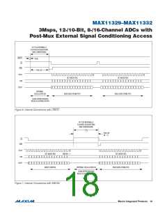
Internal Clock
Apply a soft reset when changing from internal to exter-
nal clock mode: RESET [1:0] = 10. The MAX11329–
MAX11332 operate from an internal oscillator, which
is accurate within Q15% of the 40MHz nominal clock
rate. Request internally timed conversions by writing the
appropriate sequence to the ADC Mode Control register
(Table 2).
External Clock
Apply a soft reset when changing from internal to external
clock mode: RESET [1:0] = 10. The detailed operation
of external clock mode is dependent on the mode of
operation selected for the device using SCAN[3:0] bit
settings (see Table 3). In external clock mode the analog
inputs are sampled at the falling edge of CS. Serial clock
(SCLK) is used to perform the conversion.
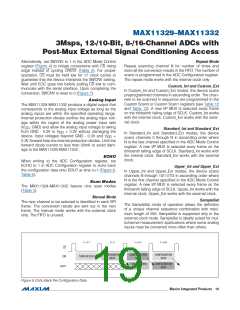
The wake-up, acquisition, conversion, and shutdown
sequences are initiated through CNVST and are per-
formed automatically using the internal oscillator. Results
are added to the internal FIFO.
With CS high, initiate a scan by setting CNVST low for
at least 5ns before pulling it high (Figure 6). Then, the
MAX11329–MAX11332 wake up, scan all requested
channels, store the results in the FIFO, and shut down.
After the scan is complete, EOC is pulled low and the
results are available in the FIFO. Wait until EOC goes
low before pulling CS low to communicate with the serial
interface. EOC stays low until CS or CNVST is pulled low
again. Do not initiate a second CNVST before EOC goes
low; otherwise, the FIFO may become corrupted.
Depending on the mode selected, the sequencer reads
in the channel to be converted from the serial data input
(DIN) at each frame (e.g. manual mode). The conversion
results are sent to the serial output (DOUT) at the next
frame.
In other external clocked modes the sequence of channel
to be converted is determined by the mode (SCAN[3:0])
selected in Table 3. See the Applications Information for
more detail on programming modes.
���������������������������������������������������������������� Maxim Integrated Products 17

 MAXIM [ MAXIM INTEGRATED PRODUCTS ]