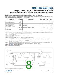
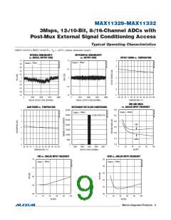
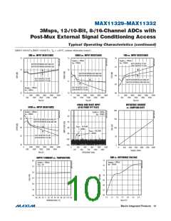
MAX11329–MAX11332
3Msps, 12-/10-Bit, 8-/16-Channel ADCs with
Post-Mux External Signal Conditioning Access
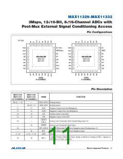
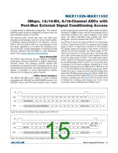
Pin Configurations
TOP VIEW
24 23 22 21 20 19 18 17
24 23 22 21 20 19 18 17
16
15
16
15
DGND 25
OVDD 26
REF-/AIN15
DGND 25
OVDD 26
REF-
CNVST/AIN14
CNVST
14 AIN
14 AIN
27
28
29
30
31
32
27
28
29
30
31
32
DOUT
EOC
DOUT
EOC
AIP
AIP
13
12
13
12
MAX11329
MAX11331
MAX11330
MAX11332
AIN0
AIN1
AIN2
AIN3
AON
AIN0
AIN1
AIN2
AIN3
AON
11 AOP
11 AOP
10
9
10
9
AIN13
AIN12
GND
GND
+
+
1
2
3
4
5
6
7
8
1
2
3
4
5
6
7
8
TQFN
16 CHANNEL
TQFN
8 CHANNEL
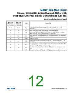
Pin Description
MAX11329
MAX11331
MAX11330
MAX11332
NAME
FUNCTION
(16 CHANNEL) (8 CHANNEL)
29–32 , 1–10
—
AIN0–AIN13 Analog Inputs
AIN0–AIN7 Analog Inputs
—
11
12
13
14
29–32, 1–4
11
12
13
14
AOP
AON
AIP
Positive Output from the Multiplexer
Negative Output from the Multiplexer
Positive Input to the ADC
AIN
Negative Input to the ADC
CNVST/
AIN14
15
—
Active-Low Conversion Start Input/Analog Input 14
—
16
15
CNVST
Active-Low Conversion Start Input
—
16
REF-/AIN15 External Differential Reference Negative Input /Analog Input 15
—
REF-
GND
External Differential Reference Negative Input
Ground
17, 19
5–10, 17, 19
External Positive Reference Input. Apply a reference voltage at REF+. Bypass to
GND with a 0.47FF capacitor.
18
18
REF+
���������������������������������������������������������������� Maxim Integrated Products 11

 MAXIM [ MAXIM INTEGRATED PRODUCTS ]