MAX11329–MAX11332
3Msps, 12-/10-Bit, 8-/16-Channel ADCs with
Post-Mux External Signal Conditioning Access
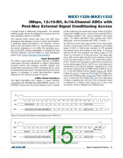
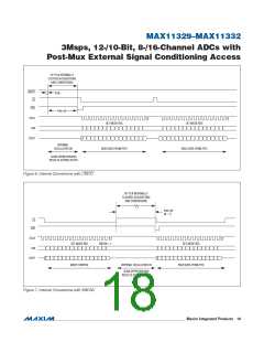
CS
1
2
3
4
5
6
7
8
9
10
11
12
13
14
15
16
SCLK
DIN
DI[15] DI[14]
DI[1] DI[0]
0
MSB] MSB-1 MSB-2
LSB
0
DOUT
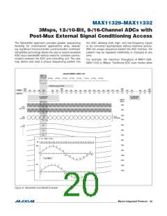
Figure 2c. External Clock Mode Timing Diagram with CHAN_ID=0
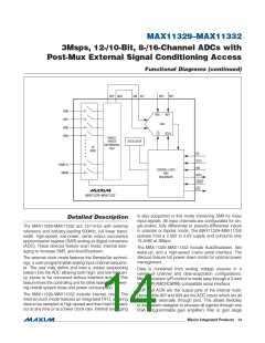
Single-Ended, Differential,
and Pseudo-Differential Input
The MAX11329–MAX11332 include up to 16 analog input
channels that can be configured on a pin-by-pin basis
to 16 single-ended inputs, 8 fully differential pairs, or 15
pseudo-differential inputs with respect to one common
input (REF-/AIN15 is the common input).
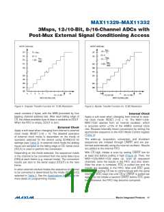
DAC
COMPARATOR
AIP
HOLD
The analog input range is 0V to V
and pseudo-differential mode (unipolar) and QV
in single-ended
REF+
AIN
(GND)
/2 or
REF+
QV
in fully differential mode (bipolar) depending on
REF+
DAC
the RANGE register settings. See Table 7 for the RANGE
register settings.
Unipolar mode sets the differential input range from 0
to V . If the positive analog input swings below the
REF+
Figure 3. Equivalent Input Circuit
negative analog input in unipolar mode, the digital output
code is zero. Selecting bipolar mode sets the differential
maximum value if the input signal exceeds this reference
range.
input range to QV
RANGE register settings (Table 7).
/2 or QV
depending on the
REF+
REF+
ADC Transfer Function
The output format of the MAX11329–MAX11332 is straight
binary in unipolar mode and two’s complement in bipolar
mode. The code transitions midway between successive
integer LSB values, such as 0.5 LSB, 1.5 LSB. Figure
4 and Figure 5 show the unipolar and bipolar transfer
function, respectively. Output coding is binary, with for
In single-ended mode, the ADC always operates in uni-
polar mode. The analog inputs are internally referenced
to GND with a full-scale input range from 0V to V
.
REF+
Single-ended conversions are internally referenced to
GND (Figure 3).
The MAX11329–MAX11332 feature up to 15 pseudo
differential inputs by setting the PDIFF_COM bits in the
Unipolar register to 1 (Table 10). The 15 analog input sig-
nals inputs are referenced to a DC signal applied to the
REF-/AIN15.
example, 1 LSB = V
as the MAX11331/MAX11332.
/4096 in the 12-bit devices such
REF+
Internal FIFO
The MAX11329–MAX11332 contain a FIFO buffer that can
hold up to 16 ADC results. This allows the ADC to handle
multiple internally clocked conversions without tying up
the serial bus. If the FIFO is filled and further conversions
are requested without reading from the FIFO, the oldest
ADC results are overwritten by the new ADC results. Each
Fully Differential Reference (REF+, REF-)
When the reference is used in fully differential mode
(REFSEL = 1), the full-scale range is set by the difference
between REF+ and REF-. The output code reaches its
���������������������������������������������������������������� Maxim Integrated Products 16

 MAXIM [ MAXIM INTEGRATED PRODUCTS ]