8- and 4-Channel, 3 ꢀ ꢁREF
Multirange Inputs, Serial 14-Bit ADCs
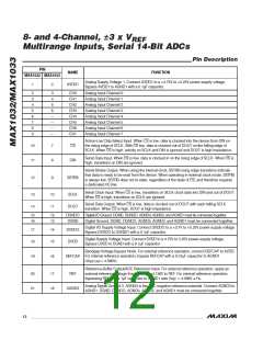
Pin Description
PIN
NAME
FUNCTION
MAX1032 MAX1033
Analog Supply Voltage 1. Connect AVDD1 to a +4.75V to +5.25V power-supply voltage.
Bypass AVDD1 to AGND1 with a 0.1µF capacitor.
1
2
AVDD1
2
3
4
5
6
7
8
9
3
4
CH0
CH1
CH2
CH3
CH4
CH5
CH6
CH7
Analog Input Channel 0
Analog Input Channel 1
Analog Input Channel 2
Analog Input Channel 3
Analog Input Channel 4
Analog Input Channel 5
Analog Input Channel 6
Analog Input Channel 7
5
6
—
—
—
—
Active-Low Chip-Select Input. When CS is low, data is clocked into the device from DIN on
the rising edge of SCLK. With CS low, data is clocked out of DOUT on the falling edge of
SCLK. When CS is high, activity on SCLK and DIN is ignored and DOUT is high impedance.
2/MAX103
10
11
7
8
CS
Serial Data Input. When CS is low, data is clocked in on the rising edge of SCLK. When CS is
high, transitions on DIN are ignored.
DIN
Serial-Strobe Output. When using the internal clock, SSTRB rising edge transitions indicate
that data is ready to be read from the device. When operating in external clock mode, SSTRB
is always low. SSTRB does not tri-state, regardless of the state of CS, and therefore requires
a dedicated I/O line.
12
9
SSTRB
Serial Clock Input. When CS is low, transitions on SCLK clock data into DIN and out of DOUT.
When CS is high, transitions on SCLK are ignored.
13
14
10
11
SCLK
DOUT
Serial Data Output. When CS is low, data is clocked out of DOUT with each falling SCLK
transition. When CS is high, DOUT is high impedance.
15
16
12
13
DGNDO
DGND
Digital I/O Ground. DGND, DGNDO, AGND3, AGND2, and AGND1 must be connected together.
Digital Ground. DGND, DGNDO, AGND3, AGND2, and AGND1 must be connected together.
Digital I/O Supply Voltage Input. Connect DVDDO to a +2.7V to +5.25V power-supply voltage.
Bypass DVDDO to DGNDO with a 0.1µF capacitor.
17
18
14
15
DVDDO
DVDD
Digital-Supply Voltage Input. Connect DVDD to a 4.75V to 5.25V power-supply voltage.
Bypass DVDD to DGND with a 0.1µF capacitor.
Bandgap-Voltage Bypass Node. For external reference operation, connect REFCAP to AVDD.
For internal reference operation, bypass REFCAP with a 0.01µF capacitor to AGND1
19
16
REFCAP
(V
REFCAP
≈ 4.096V).
Reference-Buffer Output/ADC Reference Input. For external reference operation, apply an
external reference voltage from 3.800V to 4.136V to REF. For internal reference operation,
20
21
17
18
REF
bypassing REF with a 1µF capacitor to AGND1 sets V
= 4.096V 1%.
REF
Analog Signal Ground 3. AGND3 is the ADC negative reference potential. Connect AGND3 to
AGND1. DGND, DGNDO, AGND3, AGND2, and AGND1 must be connected together.
AGND3
12 ______________________________________________________________________________________

 MAXIM [ MAXIM INTEGRATED PRODUCTS ]