DS2413: 1-Wire Dual Channel Addressable Switch
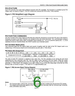
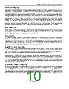
PIO STUCTURE
Each PIO consists of an open-drain pulldown transistor with 28V capability. The transistor is controlled by the PIO
Output Latch, as shown in Figure 5. The PIO Control unit connects the PIOs to the 1-Wire interface.
Figure 5. PIO Simplified Logic Diagram
PIO Pin
State
PIO Pin
PIO Output
Latch State.
PIO Data
PIO Clock
D
Q
CLOCK
Q
PIO Out-
put Latch
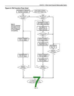
PIO FUNCTION COMMANDS
The PIO Function Flow Chart (Figure 6) describes the protocols necessary to access the PIO pins of the DS2413.
Examples on how to use these functions are included at the end of this document. The communication between
master and DS2413 takes place either at standard speed (default, OD = 0) or at Overdrive Speed (OD = 1). If not
explicitly set into the Overdrive Mode, the DS2413 powers up in standard speed.
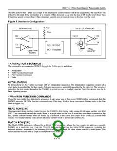
PIO ACCESS READ [F5h]
This command reads the PIO logical status and reports it together with the state of the PIO Output Latch in an
endless loop. A PIO Access Read can be terminated at any time with a 1-Wire Reset.
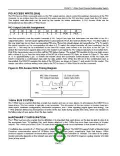
PIO Status Bit Assignment
b7
b6
b5
b4
b3
b2
b1
b0
PIOB Output
PIOB Pin
PIOA Output
PIOA Pin
Complement of b3 to b0
Latch State
State
Latch State
State
The state of both PIO channels is sampled at the same time. The first sampling occurs during the last (most
significant) bit of the command code F5h. The PIO status is then reported to the bus master. While the master
receives the last (most significant) bit of the PIO status byte, the next sampling occurs and so on until the master
generates a 1-Wire Reset. The sampling occurs with a delay of tREH+x from the rising edge of the MS bit of the
previous byte, as shown in Figure 7. The value of "x" is approximately 0.2µs.
Figure 7. PIO Access Read Timing Diagram
MS 2 bits of
LS 2 bits of PIO
Status byte
previous byte
VTH
IO
tREH+x
Sampling Point
Notes:
1
2
The "previous byte" could be the command code or the data byte resulting from the previous PIO sample.
The sample point timing also applies to the PIO Access Write command, with the "previous byte" being the
write confirmation byte (AAh).
6 of 17

 MAXIM [ MAXIM INTEGRATED PRODUCTS ]