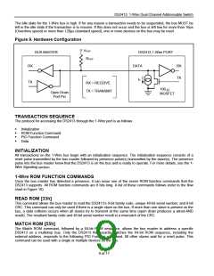
DS2413: 1-Wire Dual Channel Addressable Switch
PARAMETER
SYMBOL
CONDITIONS
Standard speed, VPUP > 4.5V
Standard speed
MIN
67.4
69.6
7.7
TYP
MAX
75
UNITS
75
Presence Detect Sample
Time (Notes 1, 20)
tMSP
µs
10
10
Overdrive speed, VPUP O 4.5V
Overdrive speed
9.1
IO PIN, 1-Wire WRITE
Standard speed, VPUP > 4.5V
Standard speed (Note 14)
Overdrive speed, VPUP O 4.5V
(Note 14)
60
62
7
120
120
16
Write-0 Low Time (Note 1)
tW0L
µs
µs
Overdrive speed (Note 14)
Standard speed
8
5
1
16
15 - ꢁ
2 - ꢁ
Write-1 Low Time
(Notes 1, 17)
tW1L
Overdrive speed
IO PIN, 1-Wire READ
Standard speed
Overdrive speed
Standard speed
Overdrive speed
5
1
Read Low Time
15 - ꢂ
2 - ꢂ
15
tRL
µs
µs
(Notes 1, 18)
Read Sample Time
(Notes 1, 18)
PIO Pins
tRL + ꢂ
tRL + ꢂ
tMSR
2
Leakage Current
Input Capacitance
Output low voltage
Input Low Voltage
Input High Voltage
(Note 21)
ILP
CP
Pin at 28V (Note 19)
(Note 5)
8.5
24
µA
pF
V
100
VOLP
VILP
20mA load current
(Note 1)
0.4
0.8
V
VPUP
–
VIHP
(Note 1)
28
V
0.3V
Note 1:
Note 2:
System requirement.
Full RPUP range guaranteed by design and simulation. not production tested. Production testing performed at a fixed RPUP value.
Maximum allowable pullup resistance is a function of the number of 1-Wire devices in the system and 1-Wire recovery times. The
specified value here applies to systems with only one device and with the minimum 1-Wire recovery times. For more heavily
loaded systems, an active pullup such as that found in the DS2482-x00, DS2480B, or DS2490 may be required.
The I-V characteristic is linear for voltages greater than 10V.
Note 3:
Note 4:
Capacitance on the data pin could be 800pF when VPUP is first applied. If a 2.2kꢀ resistor is used to pull up the data line, 2.5µs
after VPUP has been applied the parasite capacitance will not affect normal communications.
Note 5:
Note 6:
Note 7:
Note 8:
Note 9:
Note 10:
Note 11:
Note 12:
Note 13:
Note 14:
Note 15:
Guaranteed by design and simulation. Not production tested.
The voltage on IO needs to be less than or equal to VILMAX whenever the master drives the line low.
V
TL and VTH are functions of the internal supply voltage, which is a function of VPUP and the 1-Wire Recovery Times.
Voltage below which, during a falling edge on IO, a logic 0 is detected.
Voltage above which, during a rising edge on IO, a logic 1 is detected.
After VTH is crossed during a rising edge on IO, the voltage on IO has to drop by at least VHY to be detected as logic '0'.
The I-V characteristic is linear for voltages less than 1V.
Applies to a single DS2413 attached to a 1-Wire line.
The earliest recognition of a negative edge is possible at tREH after VTH has been previously reached.
Highlighted numbers are NOT in compliance with legacy 1-Wire product standards. See comparison table below.
t
PDH is deemed to have ended when the voltage on IO drops below 80% of VPUP on the leading edge of the presence-detect low
pulse. tPDL is deemed to have begun when the voltage on IO drops below 20% of VPUP on the leading edge of the pulse.
Interval during the negative edge on IO at the beginning of a Presence Detect pulse between the time at which the voltage is
Note 16:
80% of VPUP and the time at which the voltage is 20% of VPUP
.
Note 17:
Note 18:
ꢁ represents the time required for the pullup circuitry to pull the voltage on IO up from VIL to VTH
.
ꢂ represents the time required for the pullup circuitry to pull the voltage on IO up from VIL to the input high threshold of the bus
master.
Note 19:
Note 20:
The I-V characteristic is linear for voltages greater than 7V.
tMSP is a system required sample point and not directly production tested. Production testing is performed on related parameters
tPDH and tPDL. Parameter tFPD is guaranteed by design and simulation, not production tested.
Production tested for VIHP(min). VIHP(max) is guaranteed by design and simulation, not production tested.
Note 21:
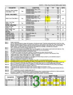
LEGACY VALUES
DS2413 VALUES
PARAMETER
STANDARD SPEED
OVERDRIVE SPEED
STANDARD SPEED
OVERDRIVE SPEED
MIN
61µs
480µs
15µs
60µs
60µs
MAX
(undef.)
(undef.)
60µs
MIN
7µs
48µs
2µs
8µs
6µs
MAX
(undef.)
80µs
MIN
67µs
600µs
15µs
60µs
62µs
MAX
(undef.)
960µs
68µs
MIN
10µs
63µs
2µs
MAX
(undef.)
80µs
tSLOT (incl. tREC
)
tRSTL
tPDH
tPDL
tW0L
6µs
8.2µs
32µs
240µs
120µs
24µs
260µs
120µs
8µs
16µs
8µs
16µs
3 of 17

 MAXIM [ MAXIM INTEGRATED PRODUCTS ]