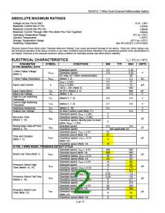
DS2413: 1-Wire Dual Channel Addressable Switch
PIN DESCRIPTION
NAME
IO
PIN #
FUNCTION
2
6
4
1
5
1-Wire bus interface. Open-drain, requires external pullup resistor.
Programmable I/O pin, open-drain with weak pulldown
Programmable I/O pin, open-drain with weak pulldown
Ground reference 1
PIOA
PIOB
GND1
GND2
Ground reference 2; both GND pins must be connected in the
application.
NC
3
Not connected
DESCRIPTION
The DS2413 combines two PIO pins and a fully featured 1-Wire interface in a single chip. PIO outputs are open-
drain, operate at up to 28V and provide an on resistance of 20ꢀ max. A robust communication protocol ensures
that PIO output changes occur error-free. Each DS2413 has a Registration Number that is 64 bits long. The
Registration Number guarantees unique identification and is used to address the device in a multidrop 1-Wire
network environment, where multiple devices reside on a common 1-Wire bus and operate independently of each
other. Device power is supplied parasitically from the 1-Wire bus. The DS2413’s applications of include accessory
identification and control, system monitoring, and general-purpose input/output.
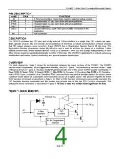
OVERVIEW
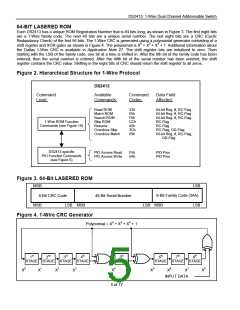
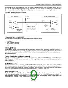
The block diagram in Figure 1 shows the relationships between the major sections of the DS2413. The DS2413
has two main components: 64-bit Registration Number, and PIO Control. The hierarchical structure of the 1-Wire
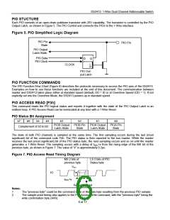
protocol is shown in Figure 2. The bus master must first provide one of the seven ROM Function Commands, 1)
Read ROM, 2) Match ROM, 3) Search ROM, 4) Skip ROM, 5) Resume, 6) Overdrive-Skip ROM or 7) Overdrive-
Match ROM. Upon completion of an Overdrive ROM command byte executed at standard speed, the device enters
Overdrive mode where all subsequent communication occurs at a higher speed. The protocol required for these
ROM function commands is described in Figure 10. After a ROM function command is successfully executed, the
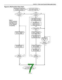
PIO functions become accessible and the master may provide one of the two PIO Function commands. The
protocol for these commands is described in Figure 6. All data is read and written least significant bit first.
Figure 1. Block Diagram
Internal VDD
PIOB
IO
1-Wire
PIO
Interface
Control
64-Bit Registration
Number
4 of 17

 MAXIM [ MAXIM INTEGRATED PRODUCTS ]