LTC6820
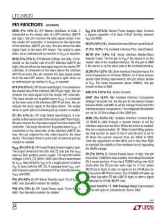
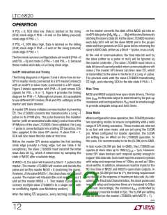
pin FuncTions (QFN/MSOP)
MOSI (Pin 1/Pin 2): SPI Master Out/Slave In Data. If
connected on the master side of a SPI interface (MSTR
pin high), this pin receives the data signal output from
the master SPI controller. If connected on the slave side
of the interface (MSTR pin low), this pin drives the data
signal input to the slave SPI device. The output is open
V
(Pin 8/Pin 9): Device Power Supply Input. Connect
DD
a bypass capacitor of at least 0.01μF directly between
and GND.
V
DD
IM (Pin 9/Pin 10): Isolated Interface Minus Input/Output.
IP (Pin 10/Pin 11): Isolated Interface Plus Input/Output.
MSTR (Pin 11/Pin 12): Serial Interface Master/Slave
drain, so an external pull-up resistor to V
is required.
DDS
Selector Input. Tie this pin to V if the device is on the
MISO (Pin 2/Pin 3): SPI Master In/Slave Out Data. If con-
nected on the master side of a SPI interface (MSTR pin
high),thispindrivesthedatasignalinputtothemasterSPI
controller. If connected on the slave side of the interface
(MSTR pin low), this pin receives the data signal output
from the slave SPI device. The output is open drain, so
DD
master side of the isolated interface. Tie this pin to GND
if the device is on the slave side of the isolated interface.
SLOW(Pin12/Pin13):SlowInterfaceSelectionInput. For
clock frequencies at or below 200kHz, or if slave devices
cannot meet timing requirements, this pin should be tied
to V . For clock frequencies above 200kHz, this pin
should be tied to GND.
an external pull-up resistor to V
is required.
DDS
DD
SCK(Pin3/Pin4):SPIClockInput/Output.Ifconnectedon
the master side of the interface (MSTR pin high), this pin
receives the clock signal from the master SPI controller.
GND (Pin 13/Pin 14): Device Ground.
ICMP (Pin 14/Pin 15): Isolated Interface Comparator
Voltage Threshold Set. Tie this pin to the resistor divider
between IBIAS and GND to set the voltage threshold of the
interfacereceivercomparators.Thecomparatorthresholds
are set to 1/2 the voltage on the ICMP pin.
This input should not be pulled above V . If connected
DDS
on the slave side of the interface (MSTR pin low), this pin
outputs the clock signal to the slave device. The output
driver is push-pull; no external pull-up resistor is needed.
CS (Pin 4/Pin 5): SPI Chip Select Input/Output. If con-
nectedonthemastersideoftheinterface(MSTRpinhigh),
thispin receives thechipselectsignalfromthemaster SPI
IBIAS (Pin 15/Pin 16): Isolated Interface Current Bias.
Tie IBIAS to GND through a resistor divider to set the
interface output current level. When the device is enabled,
this pin is approximately 2V. When transmitting pulses,
the sink current on each of the IP and IM pins is set to
20 times the current sourced from pin IBIAS to GND.
Limit the capacitance on the IBIAS pin to less than 50pF
to maintain the stability of the feedback circuit regulating
the IBIAS voltage.
controller. This input should not be pulled above V . If
DDS
connected on the slave side of the interface (MSTR pin
low), this pin outputs the chip select signal to the slave
device. The output driver is push-pull; no external pull-up
resistor is needed.
V
(Pin 5/Pin 6): SPI Input/Output Power Supply Input.
DDS
The output drivers for the SCK and CS pins use the V
DDS
EN (Pin 16/Pin 1): Device Enable Input. If high, this pin
forcestheLTC6820tostayenabled,overridingtheinternal
IDLE mode function. If low, the LTC6820 will go into IDLE
mode after the CS pin has been high for 5.7ms (when
MSTR pin is high) or after no signal on the IP/IM pins for
5.7ms(whenMSTRpinislow).TheLTC6820willwake-up
less than 8µs after CS falls (MSTR high) or after a signal
is detected on IP/IM (MSTR low).
input as their positive power supply. The input threshold
voltages of SCK, CS, MOSI, MISO and EN are determined
by V . May be tied to V or to a supply above or below
DDS
DD
V
DD
to level shift the SPI I/O. If separate from V , con-
DD
nect a bypass capacitor of at least 0.01μF directly between
and GND.
V
DDS
POL (Pin 6/Pin 7): SPI Clock Polarity Input. Tie to V or
GND. See Operation section for details.
DD
Exposed Pad (Pin 17, QFN Package Only): Exposed pad
may be left open or connected to device GND.
PHA (Pin 7/Pin 8): SPI Clock Phase Input. Tie to V or
GND. See Operation section for details.
DD
6820f
8

 Linear [ Linear ]