LTC6820
operaTion
If POL = 0, SCK idles low. Data is latched on the rising
(first) clock edge if PHA = 0 and on the falling (second)
clock edge if PHA = 1.
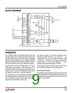
on the master converts the state of the MOSI pin into an
isoSPIdatapulse(M ,M ,…M )whilesimultaneously
N
N–1
0
latchingtheslave’sdatabit.AstheslaveLTC6820receives
each data bit it will set the slave MOSI pin to the proper
state and then generate an SCK pulse before returning the
slave’s MISO data (either as a Short –1 pulse, or as a null).
If POL =1, SCK idles high. Data is latched on the falling
(first) clock edge if PHA = 0 and on the rising (second)
clock edge if PHA = 1.
At the end of communication, the final data bit sent by
the slave (either as a pulse or null) will be ignored by
the master controller. (The slave LTC6820 must return a
data bit since it cannot predict when communications will
cease.) The master SPI device can then raise CS, which
is transmitted to the slave in the form of a Long +1 pulse.
The process ends with the slave LTC6820 transitioning
CS high, and returning SCK to the idle state if PHA = 1.
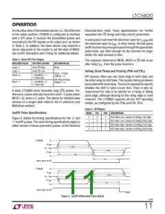
Thetwomostcommonconfigurationsaremode0(PHA= 0
and POL = 0) and mode 3 (PHA = 1 and POL = 1) because
these modes latch data on a rising clock edge.
isoSPI Interaction and Timing
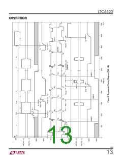
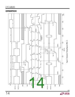
The timing diagrams in Figures 3 and 4 show how an iso-
SPI in master mode (connected to a SPI master) interacts
with an isoSPI in slave mode (connected to a SPI slave).
Figure 3 details operation with PHA = 0 (and shows SCK
signals for POL = 0 or 1). Figure 4 provides the timing
diagram for PHA = 1. Although not shown, it is acceptable
to use different SPI modes (PHA and POL settings) on the
master and slave devices.
Rise Time
MOSI and MISO outputs have open-drain drivers. The rise
time t
for the data output is determined by the pull-up
RISE
resistanceandloadcapacitance.R mustbesmallenough
PU
to provide adequate setup and hold times.
A master SPI device initiates communication by lowering
CS. The LTC6820 converts this transition into a Long –1
pulse on its IP/IM pins. The pulse traverses the isolation
barrier (with an associated cable delay) and arrives at the
IP/IM pins of the slave LTC6820. Once validated, the Long
–1 pulse is converted back into a falling CS transition, this
time supplied to the slave SPI device. If slave PHA = 1,
SCK will also leave the idle state at this time.
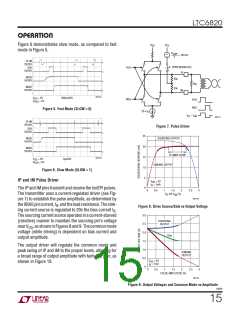
Slow Mode
Whenconfiguredforslaveoperation,theLTC6820provides
two operating modes to ensure compatibility with a wide
range of SPI timing scenarios. These modes are referred
to as fast and slow mode, and are set using the SLOW
pin. When configured for master operation, the SLOW
pin setting has no effect on the LTC6820 operation. In
this case, it is recommended to tie the SLOW pin to GND.
Before the master SPI device supplies the first latching
clock edge (usually a rising edge, but see Table 4 for
exceptions), the slave LTC6820 must transmit the initial
In fast mode (SLOW pin tied to GND), the LTC6820 can
operate at clock rates up to 1MHz (t
= 1µs). However,
CLK
slave data bit S , which it determines by sampling the
N
some SPI slave devices can’t respond quickly enough to
supportthisdatarate.Fastmoderequiresaslavetooperate
with setup and response times of 100ns, as well as 100ns
clock widths. In addition, allowances must be made for the
RC rise time of MOSI and MISO’s open-drain outputs. In
state of MISO after a suitable delay.
If MISO = 0, the slave will transmit a Short –1 pulse to the
master. The master LTC6820 will receive and decode the
pulse and set the master MISO = 0 (matching the slave).
However, if the slave MISO=1, the slave does not transmit
a pulse. The master will interpret this null response as a 1
and set the master MISO = 1. This makes it possible to
connect multiple slave LTC6820’s to a single cable with
no conflicting signals (see Multidrop section).
+
slow mode (SLOW pin tied to V ), the timing requirement
are relaxed at the expense of maximum data rate. As indi-
cated in the Electrical Characteristics, the clock pulses and
required setup and response times are increased to 0.9µs
minimum. Accordingly, the minimum t
the master) must be limited to 5µs. The SLOW pin setting
has no effect on the master LTC6820 (with MSTR = 1).
6820f
(controlled by
CLK
After the falling CS sequence, every latching clock edge
12

 Linear [ Linear ]