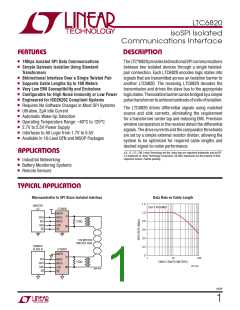
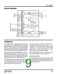
LTC6820
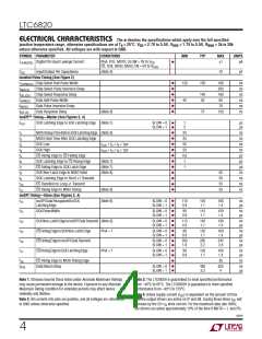
elecTrical characTerisTics The l denotes the specifications which apply over the full specified
junction temperature range, otherwise specifications are at TA = 25°C. VDD = 2.7V to 5.5V, VDDS = 1.7V to 5.5V, RBIAS = 2k to 20k
unless otherwise specified. All voltages are with respect to GND.
SYMBOL PARAMETER
CONDITIONS
MIN
TYP
MAX
UNITS
l
I
Digital Pin Input Leakage Current
PHA, POL, MSTR, SLOW = 0V to V
1
µA
LEAK(DIG)
DD
DDS
CS, SCK, MOSI, MISO, EN = 0V to V
C
Input/Output Pin Capacitance
(Note 9)
10
pF
I/O
Isolated Pulse Timing (See Figure 2)
l
l
l
l
l
l
t
t
t
t
t
t
Chip-Select Half-Pulse Width
Chip-Select Pulse Inversion Delay
Chip-Select Response Delay
Data Half-Pulse Width
Data Pulse Inversion Delay
Data Response Delay
120
40
150
180
200
190
60
70
120
ns
ns
ns
ns
ns
ns
1/2PW(CS)
INV(CS)
DEL(CS)
½PW(D)
INV(D)
140
50
(Note 8)
75
DEL(D)
isoSPI™ Timing—Master (See Figures 3, 4)
l
l
t
SCK Latching Edge to SCK Latching Edge (Note 7)
SLOW = 0
SLOW = 1
1
5
µs
µs
CLK
l
l
l
l
l
l
l
l
l
l
l
t
t
t
t
t
t
t
t
t
t
t
MOSISetupTimeBeforeSCKLatchingEdge (Note 8)
MOSI Hold Time After SCK Latching Edge
25
25
50
50
0.6
1
ns
ns
ns
ns
µs
µs
µs
ns
ns
ns
ns
1
2
SCK Low
SCK High
t
t
= t + t ≥ 1µs
3 4
3
CLK
CLK
= t + t ≥ 1µs
3 4
4
CS Rising Edge to CS Falling Edge
SCK Latching Edge to CS Rising Edge
CS Falling Edge to SCK Latch Edge
SCK Non-Latch Edge to MISO Valid
SCK Latching Edge to Short 1 Transmit
CS Transition to Long 1 Transmit
CS Rising Edge to MISO Rising
5
(Note 7)
(Note 7)
(Note 8)
6
1
7
55
50
55
55
8
9
10
11
(Note 8)
(Note 8)
isoSPI Timing—Slave (See Figures 3, 4)
l
l
t
t
t
t
t
t
isoSPIDataRecognizedtoSCK
LatchingEdge
SLOW = 0
SLOW = 1
SLOW = 0
SLOW = 1
SLOW = 0
SLOW = 1
SLOW = 0
SLOW = 1
SLOW = 0
SLOW = 1
SLOW = 0
SLOW = 1
110
0.9
90
0.9
115
0.9
90
0.9
200
1.8
90
0.9
145
1.1
115
1.1
145
1.1
120
1.1
265
2.2
120
1.1
185
1.4
150
1.4
190
1.4
160
1.4
345
2.8
160
1.4
ns
µs
ns
µs
ns
µs
ns
µs
ns
µs
ns
µs
12
13
14
15
16
17
l
l
SCKPulseWidth
l
l
SCKNon-LatchEdgetoisoSPIDataTransmit (Note 8)
l
l
CSFallingEdgetoSCKNon-LatchEdge
CSFallingEdgetoisoSPIDataTransmit
CSRisingEdgetoSCKLatchingEdge
PHA = 1
l
l
l
l
PHA = 1
l
t
t
CS Rising Edge to MOSI Rising Edge
DataReturnDelay
35
625
4
ns
ns
µs
18
l
l
SLOW = 0
SLOW = 1
485
3.3
RTN
Note 1: Stresses beyond those listed under Absolute Maximum Ratings
may cause permanent damage to the device. Exposure to any Absolute
Maximum Rating condition for extended periods may affect device
reliability and lifetime.
Note 3: The LTC6820I is guaranteed to meet specified performance
from –40°C to 85°C. The LTC6820H is guaranteed to meet specified
performance from –40°C to 125°C.
Note 4: Active supply current (I ) is dependent on the amount of time
DD
Note 2: All currents into pins are positive, and all voltages are referenced
to GND unless otherwise specified.
that the output drivers are active on IP and IM. During those times I will
DD
increase by the 20 • I drive current. For the maximum data rate 1MHz,
B
the drivers are active approximately 10% of the time if MSTR = 1, and 5%
6820f
4

 Linear [ Linear ]