LTC6820
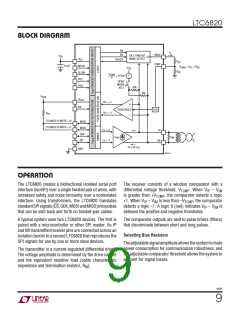
operaTion
On the other side of the isolation barrier (i.e., the other end
of the cable) another LTC6820 is configured to interface
with a SPI slave. It receives the transmitted pulses and
reconstructs the SPI signals on its output port, as shown
in Table 3. In addition, the slave device may transmit a
return data pulse to the master to set the state of MISO.
See isoSPI Interaction and Timing for additional details.
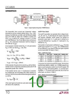
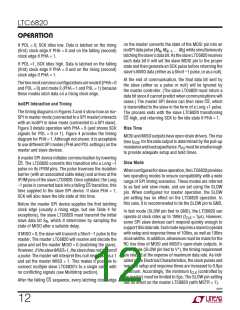
Characteristics table, these specifications are further
separated into CS (long) and Data (short) parameters.
A valid pulse must meet the minimum spec for t
and
1/2PW
the maximum spec for t . In other words, the half-pulse
INV
widthmustbelongenoughtopassthroughtheappropriate
pulse timer, but short enough for the inversion to begin
within the valid window of time.
Table 3. Slave SPI Port Output
The response observed at MOSI, MISO or CS will occur
RECEIVED PULSE
Long +1
SPI PORT ACTION
Drive CS High
Drive CS Low
RETURN PULSE
after delay t
from the pulse inversion.
DEL
None
Long –1
Setting Clock Phase and Polarity (PHA and POL)
Short –1 Pulse
if MISO = 0
Short +1
1. Set MOSI = 1
2. Pulse SCK
SPI devices often use one clock edge to latch data and
the other edge to shift data. This avoids timing problems
associatedwithclockskew.Thereisnostandardtospecify
whether the shift or latch occurs first. There is also no
requirement for data to be latched on a rising or falling
clock edge, although latching on the rising edge is most
common. The LTC6820 supports all four SPI operating
modes, as configured by the PHA and POL Pins.
(No Return Pulse
if MISO = 1)
Short –1
1. Set MOSI = 0
2. Pulse SCK
A slave LTC6820 never transmits long (CS) pulses. Fur-
thermore, aslavewillonlytransmitashort–1pulse(when
MISO = 0), never a +1 pulse. This allows for multiple slave
devices on a single cable without risk of collisions (see
Multidrop section).
Table 4. SPI Modes
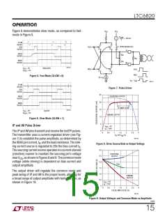
isoSPI Pulse Specifications
MODE POL
PHA DESCRIPTION
0
1
2
3
0
0
1
1
0
1
0
1
SCK Idles Low, Latches on Rising (1st) Edge
Figure 2 details the timing specifications for the +1 and
–1 isoSPI pulses. The same timing specifications apply to
either version of these symmetric pulses. In the Electrical
SCK Idles Low, Latches on Falling (2nd) Edge
SCK Idles High, Latches on Falling (1st) Edge
SCK Idles High, Latches on Rising (2nd) Edge
+1 PULSE
V
A
V
TCMP
t
1/2PW
V
– V
IP
IM
t
1/2PW
–V
TCMP
t
INV
–V
A
t
DEL
MOSI, MISO OR CS
V
–1 PULSE
A
t
INV
V
TCMP
t
1/2PW
V
– V
IP
IM
t
1/2PW
–V
TCMP
t
DEL
–V
A
MOSI, MISO OR CS
6820 F02
Figure 2. isoSPI Differential Pulse Detail
6820f
11

 Linear [ Linear ]