LTC6820
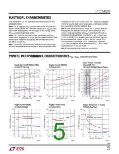
elecTrical characTerisTics
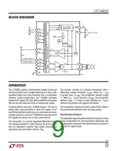
of the time if MSTR = 0. See Applications Information section for more
detailed information.
corresponds to 10m of CAT-5 cable (which has a velocity of propagation
of 66% the speed of light). Use of longer cables would require derating
these specs by the amount of additional delay.
Note 5: The IO supply pin, V , provides power for the SPI inputs and
DDS
outputs, including the EN pin. If the inputs are near 0V or V
(to avoid
Note 8: These specifications do not include rise or fall time. While fall
time (typically 5ns due to the internal pull-down transistor) is not a
DDS
static current in input buffers) and the outputs are not sourcing current,
then I includes only leakage current.
concern, rising-edge transition time t
is dependent on the pull-up
DDS
RISE
resistance and load capacitance. In particular, t and t require t
12
14
RISE
Note 6: The LTC6820 is guaranteed to meet specifications with R
resistor values ranging from 2k to 20k, with 1% or better tolerance. Those
BIAS
< 110ns (if SLOW = 0) for the slave’s setup and hold times. Therefore,
the recommended time constant is 50ns or less. For example, if the
total capacitance on the data pin is 25pF (including self capacitance
resistor values correspond to a typical I that can range from 0.1mA
B
(for 20k) to 1mA (for 2k).
Note 7: These timing specifications are dependent on the delay through
the cable, and include allowances for 50ns of delay each direction. 50ns
C
I/O
of 10pF), the required pull-up resistor value is R ≤ 2kΩ. If these
PU
requirements can’t be met, use SLOW = 1.
Note 9: Guaranteed by design. Not tested in production.
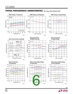
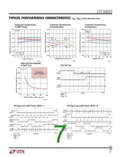
Typical perForMance characTerisTics V
DD = VDDS, unless otherwise noted.
Input Voltage Threshold
(Except EN Pin)
Supply Current (READY/ACTIVE)
vs Clock Frequency
Supply Current (READY)
vs Temperature
vs Supply Voltage (VDD or VDDS
4.0
)
5.3
5.2
5.1
5.0
4.9
4.8
7
6
I
= 1mA
B
3.5
V
= 5V, I = 1mA
B
DD
ONLY
SPI PINS
3.0
2.5
2.0
1.5
1.0
0.5
0
V
= 3V, I = 1mA
B
HIGH
DD
V
= 5V
DD
V
5
4
IH
LOW
V
= 3V
DD
3
2
1
V
= 5V, I = 0.1mA
B
DD
V
IL
V
= 3V, I = 0.1mA
B
DD
MSTR = 1
200
–50 –25
0
25
50
75 100 125
0
400
600
800
1000
1.5 2.0 2.5 3.0 3.5 4.0 4.5 5.0 5.5
SUPPLY VOLTAGE (V)
FREQUENCY (kHz)
TEMPERATURE (°C)
6820 G01
6820 G02
6820 G03
Supply Current (IDLE)
vs Supply Voltage
Supply Current (IDLE)
vs Temperature
Output Resistance vs Supply
Voltage (VOH/VOL
)
3.0
2.5
2.0
1.5
1.0
0.5
0
3.0
2.5
2.0
1.5
1.0
0.5
0
100
80
60
40
20
0
V
DD
= 5V
OUTPUT
SOURCING 2mA CURRENT
SLAVE (MSTR = 0)
SLAVE (MSTR = 0)
MASTER (MSTR = 1)
MASTER (MSTR = 1)
OUTPUT SINKING 3.3mA CURRENT
2.5
3.5
4.0
4.5
5.0
5.5
3.0
50
TEMPERATURE (°C)
100 125
2.5
3.5
4.5
–50 –25
0
25
75
1.5
5.5
SUPPLY VOLTAGE (V)
SUPPLY VOLTAGE (V)
6820 G04
6820 G05
6820 G19
6820f
5

 Linear [ Linear ]