LTC6820
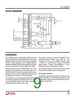
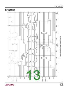
block DiagraM
EN
CS
I
B
IBIAS
ICMP
IDLE TIMEOUT
WAKE DETECT
V
DD
2V
V
READY
DD
R
R
B1
0.1µF
MSTR
SLOW
POL
R
= R + R
B1 B2
BIAS
V
DD
B2
V
ICMP
3
+
+ 167mV
–
OPEN
WHEN
IDLE
PHA
35k
35k
V
DDS
V
DDS
Rx = +1
Rx = –1
+
EN
THRESHOLD
0.5x
R
PU
–
(TO MOSI IF MSTR = 0)
(TO MISO IF MSTR = 1)
MOSI
MISO
SCK
CS
Tx = +1
Tx = –1
IP
I
R
M
DRV
IM
Tx • 20 • I
B
GND
6820 BD
operaTion
The LTC6820 creates a bidirectional isolated serial port
interface (isoSPI) over a single twisted pair of wires, with
increased safety and noise immunity over a nonisolated
interface. Using transformers, the LTC6820 translates
standardSPIsignals(CS,SCK,MOSIandMISO)intopulses
that can be sent back and forth on twisted-pair cables.
The receiver consists of a window comparator with a
differential voltage threshold, V . When V – V
TCMP
IP
IM
is greater than +V
, the comparator detects a logic
TCMP
+1. When V – V is less than –V , the comparator
IP
IM
TCMP
detects a logic –1. A logic 0 (null) indicates V – V is
IP
IM
between the positive and negative thresholds.
A typical system uses two LTC6820 devices. The first is
paired with a microcontroller or other SPI master. Its IP
and IM transmitter/receiver pins are connected across an
isolation barrier to a second LTC6820 that reproduces the
SPI signals for use by one or more slave devices.
The comparator outputs are sent to pulse timers (filters)
that discriminate between short and long pulses.
Selecting Bias Resistors
Theadjustablesignalamplitudeallowsthesystemtotrade
power consumption for communication robustness, and
the adjustable comparator threshold allows the system to
account for signal losses.
The transmitter is a current-regulated differential driver.
The voltage amplitude is determined by the drive current
and the equivalent resistive load (cable characteristic
impedance and termination resistor, R ).
M
6820f
9

 Linear [ Linear ]