LTC6820
operaTion
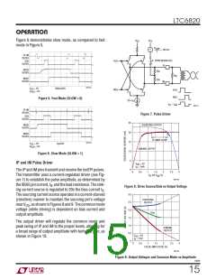
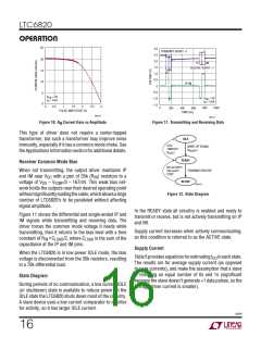
Figure 6 demonstrates slow mode, as compared to fast
mode in Figure 5.
V
V
DD
DD
V
ICMP
3
+
+ 167mV
–
IP-IM
2V/DIV
SCK
OPEN WHEN IDLE
IP
POS
5V/DIV
MOSI
5V/DIV
35k
R
M
MISO
5V/DIV
35k
IM
6820 F05
V
V
= 5V
DDS
200ns/DIV
DD
NEG
POS
NEG
= 5V
Figure 5. Fast Mode (SLOW = 0)
20 • I
B
V
IP
– V
IM
6820 F07
IP-IM
2V/DIV
SCK
5V/DIV
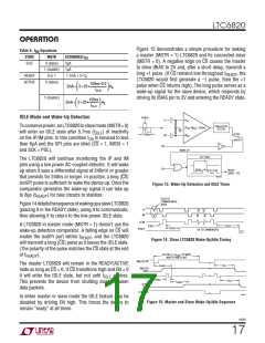
Figure 7. Pulse Driver
25
20
15
10
MOSI
SOURCING OUTPUT
5V/DIV
MISO
5V/DIV
1V AMPLITUDE
6820 F06
V
V
= 5V
DDS
1µs/DIV
DD
= 5V
SINKING OUTPUT
Figure 6. Slow Mode (SLOW = 1)
5
0
IP and IM Pulse Driver
V
B
= 3V
DD
= 1mA
I
The IP and IM pins transmit and receive the isoSPI pulses.
The transmitter uses a current-regulated driver (see Fig-
ure 7) to establish the pulse amplitude, as determined by
0
1
V
1.5
2
2.5
3
0.5
OR V (V)
IP
IM
6820 F08
theIBIASpincurrent, I , andtheloadresistance. Thesink-
B
Figure 8. Drive Source/Sink vs Output Voltage
ing current source is regulated to 20x the bias current I .
B
3.0
The sourcing current source operates in a current-starved
SOURCING
OUTPUT
(resistive) manner to maintain the sourcing pin’s voltage
2.5
2.0
1.5
1.0
0.5
0
nearV , asshowninFigures8and9. Thecommonmode
DD
voltage (while driving) is dependent on bias current and
V
CM
output amplitude.
The output driver will regulate the common mode and
peak swing of IP and IM to the proper levels, allowing for
a broad range of output amplitude with fairly flat gain, as
shown in Figure 10.
SINKING
OUTPUT
V
I
= 3V
DD
= 1mA
B
0
1
1.5
2
2.5
3
0.5
PULSE AMPLITUDE (V)
6820 F09
Figure 9. Output Voltages and Common Mode vs Amplitude
6820f
15

 Linear [ Linear ]