LTC6820
operaTion
25
3.0
2.5
2.0
1.5
1.0
0.5
0
TRANSMIT SHORT +1
20
15
10
5
IP
IM
RECEIVE SHORT –1
IP-IM
–0.5
–1.0
V
S
= 3V
DD
V
B
= 3V
DD
I
= 1mA
I
= 1mA
0
–1.5
0
1
1.5
2
2.5
3
0.5
0
800
1000
200
400
TIME (ns)
600
PULSE AMPLITUDE (V)
6820 F10
6820 F11
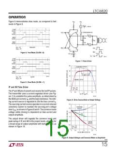
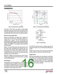
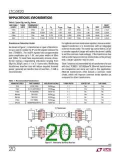
Figure 10. AIB Current Gain vs Amplitude
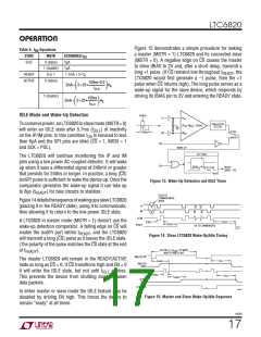
Figure 11. Transmitting and Receiving Data
This type of driver does not require a center-tapped
transformer, but such a transformer may improve noise
immunity, especially if it has a common mode choke. See
theApplicationsInformationsectionforadditionaldetails.
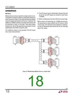
IDLE
IDLE
WAKE-UP SIGNAL
(t
TIMEOUT
)
READY
(t
IDLE
)
READY
Receiver Common Mode Bias
NO ACTIVITY
ON isoSPI
PORT
TRANSMIT/RECEIVE
When not transmitting, the output driver maintains IP
and IM near V with a pair of 35k (R ) resistors to a
DD
IN
ACTIVE
voltage of V – V
/3 – 167mV. This weak bias net-
ICMP
DD
6820 F12
work holds the outputs near their desired operating point
withoutsignificantlyloadingthecable,whichallowsalarge
number of LTC6820’s to be paralleled without affecting
signal amplitude.
Figure 12. State Diagram
In the READY state all circuitry is enabled and ready to
transmit or receive, but is not actively transmitting on IP
and IM.
Figure 11 shows the differential and single-ended IP and
IM signals while transmitting and receiving data. The
driver forces the common mode voltage it needs while
transmitting, then it returns to the bias level with a time
Supply current increases when actively communicating,
so this condition is referred to as the ACTIVE state.
constant of R • C
/2, where C
is the sum of the
IN
LOAD
LOAD
capacitance at the IP and IM pins.
Supply Current
When the LTC6820 is in low power IDLE mode, the bias
voltage is disconnected from the 35k resistors, resulting
in a 70k differential load.
Table5providesequationsforestimatingI ineachstate.
DD
The results are for average supply current (as opposed
to peak currents), and make the assumption that a slave
is returning an equal number of 0s and 1s (significant
because the slave doesn’t generate +1 data pulses, so the
average driver current is smaller).
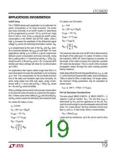
State Diagram
During periods of no communication, a low current IDLE
(or shutdown) state is available to reduce power. In the
IDLE state the LTC6820 shuts down most of the circuitry.
A slave device uses a low current comparator to monitor
for activity, so it has larger IDLE current.
6820f
16

 Linear [ Linear ]