LTC4270/LTC4271
APPLICATIONS INFORMATION
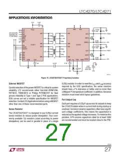
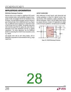
ESD/Cable Discharge Protection
LAYOUT GUIDELINES
Ethernet ports can be subject to significant ESD events
when long data cables, each potentially charged to thou-
sands of volts, are plugged into the low impedance of the
RJ45jack. Toprotectagainstdamage, eachportrequiresa
Strict adherence to board layout, parts placement and
routing guidelines is critical for optimal current read-
ing accuracy, IEEE compliance, system robustness, and
thermal dissipation. Refer to the DC1682A Demo Board
as a layout reference. Contact LTC Applications to obtain
a full set of layout guidelines, example layouts and BOMs.
pair of clamp diodes; one to AGND and one to V (Figure
EE
16). An additional surge suppressor is required for each
LTC4270 chip from V to AGND. The diodes at the ports
EE
steer harmful surges into the supply rails, where they are
0.22μF
S1B
A
PORTn
GND
absorbed by the surge suppressor and the V bypass
EE
OUTn
capacitance. The surge suppressor has the additional
LTC4270
SMAJ58A
–54V
0.1μF
benefit of protecting the LTC4270 from transients on the
GATEn
V
supply.
S1B
EE
SENSEn
V
S1B diodes work well as port clamp diodes, and an
EE
0.25Ω
SMAJ58AorequivalentisrecommendedfortheV surge
EE
42701 F17
suppressor.
Figure 16. LTC4270 Discharge Protection
42701f
28

 Linear [ Linear ]