LTC4270/LTC4271
APPLICATIONS INFORMATION
For simple devices such as small PoE switches, the isola-
tion requirement can be met by using an isolated main
power supply for the entire device. This strategy can be
used if the device has no electrically conducting ports
other than twisted-pair Ethernet. In this case, the SDAIN
and SDAOUT pins can be tied together and will act as a
In the LTC4270/LTC4271, V should be delivered by the
DD
host controller’s non-isolated 3.3V supply. To maintain
required isolation AGND and DGND must not be con-
nected in any way.
Main PoE Power Supply
2
standard I C/SMBus SDA pin.
V
EE
is the main isolated PoE supply that provides power
to the PDs. Because it supplies a relatively large amount
of power and is subject to significant current transients,
it requires more design care than a simple logic supply.
If the device is part of a larger system, contains additional
external non-Ethernet ports, or must be referenced to
protective ground for some other reason, the Power over
Ethernet subsystem must be electrically isolated from the
rest of the system.
For minimum IR loss and best system efficiency, set V
EE
near maximum amplitude (57V), leaving enough margin
to account for transient over or undershoot, temperature
drift, andthelineregulationspecificationsoftheparticular
power supply used.
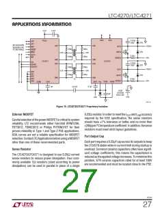
The LTC4270/LTC4271 chipset simplifies PSE isolation by
allowing the LTC4271 chip to reside on the non-isolated
side. There it can receive power from the main logic sup-
2
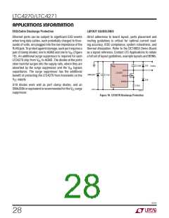
Bypass capacitance between AGND and V is very im-
ply and connect directly to the I C/SMBus bus. Isolation
EE
portant for reliable operation. If a short circuit occurs at
one of the output ports it can take as long as 1ꢀs for the
LTC4270 to begin regulating the current. During this time
the current is limited only by the small impedances in the
circuit and a high current spike typically occurs, causing a
between the LTC4271 and LTC4270 is implemented using
aproprietarytransformer-basedcommunicationprotocol.
Additional details are provided in the Serial Bus Isolation
section of this data sheet.
voltage transient on the V supply and possibly causing
EE
EXTERNAL COMPONENT SELECTION
the LTC4270/LTC4271 to reset due to a UVLO fault. A 1ꢀF,
100V X7R capacitor placed near the V pin along with an
EE
Power Supplies and Bypassing
electrolyticbulkcapacitorofatleast47μFisrecommended
The LTC4270/LTC4271 requires two supply voltages to
to minimize spurious resets.
operate. V requires 3.3V (nominally) relative to DGND.
DD
V
EE
requires a negative voltage of between –44V and
Serial Bus Isolation
–57V for Type 1 PSEs, –50V to –57V for Type 2 PSEs,
TheLTC4270/LTC4271chipsetusestransformerstoisolate
the LTC4271 from the LTC4270. In this case, the SDAIN
and SDAOUT pins can be shorted to each other and tied
++
or –54.75V to –57V for LTPoE PSEs, relative to AGND.
Digital Power Supply
2
directly to the I C/SMBus bus. The transformers should
V
provides digital power for the LTC4271 processor,
DD
be 10BASE-T or 10/100BASE-T with a 1:1 turns ratio. It
is important that the selected transformers do not have
common-mode chokes. These transformers typically
provide 1500V of isolation between the LTC4271 and the
LTC4270. For proper operation strict layout guidelines
must be met.
and draws a maximum of 15mA. A ceramic decoupling
cap of at least 0.1ꢀF should be placed from V to DGND,
DD
as close as practical to each LTC4271 chip. A 1.8V core
voltage supply is generated internally and requires a 1μF
ceramic decoupling cap between the CAP1 pin and DGND.
42701f
26

 Linear [ Linear ]