LTC3649
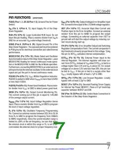
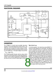
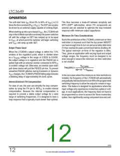
FUNCTIONAL DIAGRAM
BOOST
V
IN
INTV
EXTV
CC
CC
1/50k
PEAK
CURRENT
REVERSE
COMPARATOR
V
IN
COMPARATOR
LDO
–
+
0A
+
–
50µA
+
–
ISET
IMON
V
1/40k
+
OUT
ITH
SW
BUCK LOGIC
–
+
INTV
PGDFB
PGOOD
CC
AND
2V
2V
+
–
GATE DRIVE
V
INREG
PGOOD
LOGIC
MODE/SYNC
CLK
OSC
R
T
RUN
SGND
PGND
3649 FD
OPERATION
The LTC3649 is a current mode monolithic step-down
Main Control Loop
regulator. The accurate 50µA bias current on the I pin
SET
In normal operation, the internal top power MOSFET is
turned on at the beginning of a clock pulse. The inductor
current is allowed to ramp up to a peak level. Once that
level is reached, the top power switch is turned off and
the bottom switch is turned on until the next clock cycle.
The peak inductor current is determined by sensing the
allows the user to program the output voltage in a unity-
gain buffer fashion with just one external resistor from the
I
pin to GND (R ). The output voltage is set such that:
SET
SET
V
OUT
= 50µA • R
SET
The LTC3649 operates through a wide V range, and its
IN
voltagedropacrosstheSWandV nodesofthetoppower
IN
frequency can be programmed to a wide range with the R
T
MOSFET. The voltage on the ITH pin sets the comparator
thresholdcorrespondingtoinductorpeakcurrent.Theerror
amplifier, EA, adjusts this ITH voltage by comparing the
resistor. To suit a variety of applications, the MODE/SYNC
pin allows the user to trade off output ripple for efficiency.
V
voltage with the voltage on ISET. If the load current
OUT
increases, it causes a drop in V
relative to V . This
OUT
ISET
causes the ITH voltage to rise until the average inductor
current matches that of the load current.
3649fb
8
For more information www.linear.com/LTC3649

 Linear [ Linear ]