LTC3649
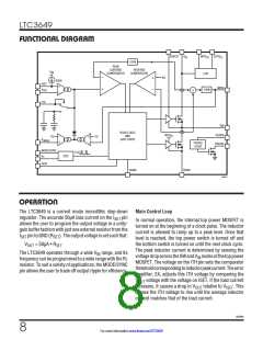
OPERATION
the input to hold the input voltage at the regulated point.
The regulator will continue to perform this operation until
the output capacitor has dissipated so much energy that it
can no longer hold up the input voltage. This momentary
input voltage holdup proves to be a handy tool for certain
applications.
rising threshold (1.2V), and the regulator will turn on.
Similarly,onceon,iftheinputvoltagedecreasesbelowthe
RUN
V
falling threshold (1.1V), the regulator will turn off.
V Overvoltage Protection
IN
In order to protect the internal power MOSFET devices
against transient voltage spikes, the LTC3649 constantly
INTV Regulator
CC
monitors the V pin for an overvoltage condition. When
IN
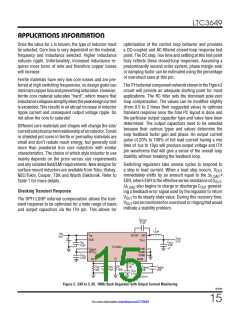
TheLTC3649hastwoonboardinternallowdropout(LDO)
regulatorsthatpowerthedriversandinternalbiascircuitry.
Regardless of which one is in operation, the INTV must
be bypassed to GND with a minimum of 2.2µF ceramic
capacitor. Good bypassing is necessary to supply the
high transient current required by the power MOSFET
gate drivers.
V
rises above 70V, the regulator suspends operation
IN
by shutting off both power MOSFETs and discharges the
ISET pin voltage to ground. Once V drops below the
CC
IN
V
threshold, the regulator resumes normal switching
OVLO
operation.
Programming Switching Frequency
Connecting a resistor from the R pin to GND programs
The first LDO is powered from V , and the INTV volt-
T
IN
CC
the switching frequency from 300kHz to 3MHz according
age is regulated to 3.3V. The power dissipated across
to the following formula:
this LDO would thus equal to (V – 3.3) • I
. For
IN
INTVCC
a typical 1MHz application running in CCM, the current
105
RT(kΩ)
drawn from INTV by the chip is roughly 20mA. Thus,
f (kHz)=
CC
if the input voltage is high, the power loss and heat rise
due to this LDO is significant.
Do not float the R pin.
T
Tocombatthisissue,aseparateLDOexiststhatispowered
Theinternalphase-lockedloophasasynchronizationrange
of 508 around its programmed frequency. Therefore,
from EXTV . As long as the input voltage is above 5V
CC
and the EXTV voltage is above 3.2V, this LDO will take
duringexternalclocksynchronization, theproperR value
CC
T
over and regulate the INTV voltage to 3.1V. In applica-
should be selected such that the external clock frequency
CC
tions where the output voltage is programmed to 3.3V or
iswithinthis508rangeoftheR programmedfrequency.
T
above, it is recommended that the V
(<2ꢀV) pin be
OUT
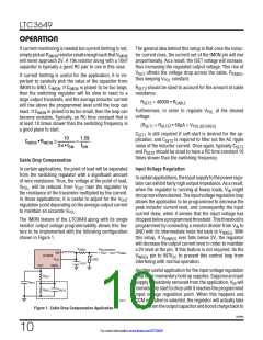
Output Voltage Tracking and Soft-Start
directly tied to the EXTV pin. Otherwise, if a separate
CC
lower voltage rail exists on board that can supply INTV
CC
TheLTC3649allowstheusertoprogramitsoutputvoltage
current, then attaching that supply to EXTV will also
CC
ramp rate by means of the ISET pin. Since V
servos
OUT
suffice provided that a 1µF ceramic bypass capacitor is
its voltage to that of V , placing an external capacitor
ISET
placed from the EXTV pin to GND physically close to
CC
C
from the ISET pin to GND will program the ramp-up
rate of the ISET pin and thus the V
SET
the chip. Both examples should significantly reduce the
voltage.
OUT
power loss through the LDO.
1
t
•C
VOUT(t)=IISET •RSET 1−eRSET SET
V Undervoltage Programming
IN
LTC3649 offers an accurate RUN threshold to start the
regulator. As a result, a resistor divider from IN to GND
can be placed with the intermediate node fed back to RUN
From 08 to 908 V
:
OUT
tosetanaccurateV undervoltagethreshold. Astheinput
IN
t
SS
t
SS
≅ –R • C • In(1 – 0.9)
SET SET
voltagerises,theRUNvoltagewillincreaseabovetheV
RUN
≅ 2.3 • R • C
SET
SET
3649fb
11
For more information www.linear.com/LTC3649

 Linear [ Linear ]