LTC3649
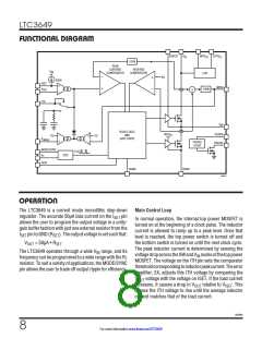
OPERATION
Low Current Operation
set the output voltage, the 50µA of current out of the ISET
pin is only guaranteed to be accurate when V
is more
ISET
Burst Mode operation can be selected by connecting the
MODE/SYNC pin to GND. In this mode, the LTC3649 will
automatically transition from continuous mode operation
to Burst Mode operation when the load current is low. A
reversecurrentcomparatorlooksatthevoltageacrossSW
to GND and turns off the bottom power MOSFET when
that voltage difference approaches zero. This prevents the
inductor current from going negative. An internal burst
clamp is set to be approximately 1A, which means that in
BurstModeoperation, thepeakinductorcurrentwillnever
go below 1A regardless of what the ITH voltage demands
the peak current to be. As a result, when the load is low
than 500mV below V . As the input voltage drops below
IN
that500mVthreshold, theISETcurrentwilldecrease, thus
limitingtheprogrammedvoltage.Typically,V
willnever
OUT
ISET
get within 300mV of V . Since V
programs V , this
IN
ISET
limitation essentially enforces a maximum duty cycle for
the switcher. This limitation can be overcome if an accu-
rate external supply is used to drive the ISET pin directly.
The second limitation against full dropout operation
is the requirement for the BOOST to SW capacitor to
refresh. When the top power MOSFET is on for multiple
clock cycles during dropout operation, the BOOST to SW
capacitor slowly gets depleted by the internal circuitry of
the chip. When the bottom switch does not turn on for at
least ꢀ0ns for ꢀ periods, it is forced to turn on in order to
guarantee sufficient voltage on the bootstrap capacitor.
During a refresh, the bottom switch will only turn on for
roughly 308 of the period to limit inductor ripple, thus
limiting output voltage ripple.
enough,V willriserelativetoV
becausetheaverage
OUT
ISET
programmed inductor current is above the load current,
thusdrivingV low. OncetheITHvoltageisdrivenbelow
ITH
an internal threshold (~400mV), the switching regulator
will enter its sleep mode and wait for V
to drop and
OUT
V
ITH
to rise above the threshold before it starts to switch
again. During sleep mode, the quiescent current of the
part is reduced to less than 400µA to conserve input
power. The LTC3649 is designed to operate with single
burst pulse behavior to minimize output voltage ripple
while keeping the efficiency high at light loads. Lastly, if
at any point the top power MOSFET is on for roughly ꢀ
consecutive clock cycles, the part will turn on the bottom
power MOSFET for a brief duration such that the BOOST
capacitor can be replenished.
Output Current Monitoring and Regulation
The LTC3649 has the ability to accurately sense the aver-
age inductor current without the use of an external sense
resistor. The IMON pin output current is 1/40000th scale
of the inductor current. Placing a resistor from IMON to
GND allows the voltage on that node to be equal to:
RIMON •IL
40000
V
=
IMON
Forced Continuous Mode Operation
Floating the MODE/SYNC pin defaults the LTC3649 into
forced continuous mode operation. In this mode, the
part switches continuously regardless of load current,
and the inductor peak current is allowed to decrease to
approximately –1A to allow for negative average current.
Since the IMON current mirrors the inductor current, it
is necessary to place a capacitor from IMON to GND to
filter the voltage on the node. The choice of this capacitor
is discussed below.
In addition to simply sensing the inductor current, the
LTC3649 can also be programmed to regulate the aver-
age output current limit. The regulator will limit the peak
inductor current if it senses that the voltage on IMON
has exceeded 2V. As a result, the programmed average
High Duty Cycle/Dropout Operation
As the input voltage decreases towards the desired output
voltage, the duty cycle will increase towards 1008. How-
ever, given the architecture, there are two restrictions that
prevent the LTC3649 from operating in full dropout mode.
inductor current depends on the size of R
such that:
IMON
2V • 40000
ILAVG
=
The first restriction is due to how the ISET voltage is pro-
grammed. If a resistor is placed between ISET and GND to
RIMON
3649fb
9
For more information www.linear.com/LTC3649

 Linear [ Linear ]