LTC3649
ELECTRICAL CHARACTERISTICS
Note 1: Stresses beyond those listed under Absolute Maximum Ratings
may cause permanent damage to the device. Exposure to any Absolute
Maximum Rating condition for extended periods may affect device
reliability and lifetime.
0°C to ꢀ5°C junction temperature. Specifications over the –40°C to
125°C operating junction temperature range are assured by design,
characterization and correlation with statistical process controls. The
LTC3649I is guaranteed over the full –40°C to 125°C operating junction
temperature range. Note that the maximum ambient temperature
consistent with these specifications is determined by specific operating
conditions in conjunction with board layout, the rated package thermal
impedance and other environmental factors.
Note 2: All voltages are referred to V
/V
.
SGND PGND
Note 3: Transient absolute maximum voltages should not be applied for
more than 48 of the switching duty cycle.
Note 4: V
can be programmed to V if the ISET pin is driven to that
IN
OUT
Note 6: The quiescent current in FC mode does not include switching loss
of the power FETs.
voltage. If a resistor is used to program V , the current into the ISET pin
ISET
will decrease as V
approaches V . Refer to the ISET current vs V
ISET
IN ISET
Note 7: This IC includes overtemperature protection that is intended
to protect the device during momentary overload conditions. Junction
temperature will exceed 125°C when overtemperature protection is active.
Continuous operation above the specified maximum operating junction
temperature may impair device reliability.
graph as an example and reference. Furthermore, during high I
and
OUT
high duty cycle operation, V
may be limited by the voltage drop across
OUT
the top switch. Refer to the High Duty Cycle/Dropout Operation section for
more details.
Note 5: The LTC3649 is tested under pulsed load conditions such that
T ≈ T . The LTC3649E is guaranteed to meet specifications from
J
A
TA = 25°C, unless otherwise noted.
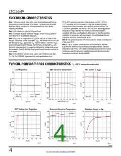
TYPICAL PERFORMANCE CHARACTERISTICS
Load Regulation
ISET Current vs Temperature
ISET Current vs VISET
51
50
49
48
47
46
50.5
50.3
50.1
49.9
49.7
49.5
102
101
100
99
FC MODE
BM
V
V
= 24V
= 5V
IN
OUT
V
= 24V
4
IN
98
–55 –35 –15
5
25 45 65 85 105 125
0
1
2
3
4
0
8
12
16
20
24
TEMPERATURE (°C)
I
(A)
V
ISET
OUT
3649 G02
3649 G01
3649 G03
ISET Voltage Line Regulation
Quiescent Current vs Temperature
Shutdown Current vs VIN
5.01
5.00
4.99
4.97
4.96
4.95
20
16
12
8
500
400
300
200
100
0
SLEEP
4
SHUTDOWN
R
= 100kΩ
50 60
ISET
0
0
10
20
30
(V)
40
–55 –35 –15
5
25 45 65 85 105 125
0
10
20
30
(V)
40
50
60
V
TEMPERATURE (°C)
V
IN
IN
3649 G04
3649 G05
3649 G06
3649fb
4
For more information www.linear.com/LTC3649

 Linear [ Linear ]