LTC3649
PIN FUNCTIONS (QFN/TSSOP)
PGND(Pins1, 2, 26-28/Pins1-5):GroundPinsforPower
Switch.
V
(Pin13/Pin16):OutputVoltageErrorAmplifierInput
OUT
Pin.ConnecttotheoutputoftheLTC3649voltageregulator.
V
(Pin 3, 4/Pins 6, 7): Input Supply Pin of the Step-
ISET (Pin 14/Pin 17): Accurate 50µA Bias Current and
Positive Input to the Error Amplifier. Connect an external
resistor from this pin to SGND to program the output
voltage. Connecting an external capacitor from ISET to
ground will soft start the output voltage by reducing cur-
rent inrush during start-up.
IN
Down Regulator.
RUN (Pin 5/Pin 8): Logic Controlled RUN Input. Do not
leave this pin floating. Place a resistor divider from V to
IN
GND for an accurate V undervoltage threshold.
IN
SGND (Pins 6, 29/Pins 9, 29): Signal Ground Pin of the
Step-Down Regulator. The exposed pad must be soldered
to PCB ground for electrical connection and rated thermal
performance.
ITH (Pin 15/Pin 18): Error Amplifier Output and Switching
Regulator Compensation Point. The current comparator’s
trip threshold is linearly proportional to this voltage. Tying
this pin to INTV activates internal compensation.
CC
MODE/SYNC (Pin 7/Pin 10): Mode Select and Oscillator
Synchronization Input of the Step-Down Regulator. Leave
MODE/SYNC floating for forced continuous mode opera-
tion or tie MODE/SYNC to GND for Burst Mode operation.
Furthermore,connectingMODE/SYNCtoanexternalclock
willsynchronizetheinternaloscillatortotheexternalclock
signal and put the part in forced continuous mode.
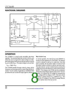
EXTV (Pin 16/ Pin 19): External Power Input to the
CC
Internal Regulator. The internal regulator will draw cur-
rent from EXTV instead of V when EXTV is tied to a
CC
IN
CC
voltage higher than 3.2V and V is above 5V. For output
IN
voltages at or above 3.3V and less than 2ꢀV, this pin can
be tied to V . If this pin is tied to a supply other than
OUT
V
, locally bypass with at least a 1µF to GND.
OUT
PGOOD (Pin 8/Pin 11): V
Within Regulation Indicator.
OUT
INTV (Pin 17/Pin 20): Low Dropout Regulator. Locally
CC
PGOOD is pulled to GND when V
or less than 0.555V.
is more than 0.645V
PGFB
bypass with at least 2.2µF to GND.
BOOST (Pin 18/Pin 21): Boosted Floating Driver Supply
for Internal Top Power MOSFET. Place a 0.1µF bootstrap
capacitor between BOOST and SW.
PGDFB(Pin9/Pin12):PowerGoodFeedback.Placearesis-
tor divider from V to GND to detect power good level.
OUT
IMON (Pin 10/Pin 13): Output Current Monitoring Pin.
The current coming out of this pin is equal to 1/40,000
of the average output current.
SW (Pins 19-25/Pins 22-28): Switch Node Connection to
the Inductor of the Step-Down Regulator.
V
(Pin 11/Pin 14): Input Voltage Regulation Sense
INREG
Input. Place a resistor divider from V to GND to program
IN
the level of input voltage regulation.
R (Pin 12/Pin 15): Oscillator Frequency Programming
T
Pin. Connect an external resistor between 333.3k to 33.3k
from R to GND to program the frequency from 300kHz
T
to 3MHz respectively. Since the synchronization range is
limited to 508 of the set frequency, be sure that either
the external clock is within this range or R is set to ac-
T
commodate the external clock for proper frequency lock.
3649fb
7
For more information www.linear.com/LTC3649

 Linear [ Linear ]