LTC3649
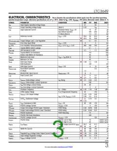
ELECTRICAL CHARACTERISTICS The l denotes the specifications which apply over the specified operating
junction temperature range, otherwise specifications are at TJ = 25°C. (Note 5) VIN = 24V, VEXTVCC = 0V unless otherwise noted. (Notes 5, 7)
SYMBOL
PARAMETER
CONDITIONS
MIN TYP
3.1
0.05
MAX
60
V
IN
30
600
2.5
UNITS
V
V
Input Supply Operating Voltage Range
Output Operating Voltage Range
Input Quiescent Current
V
V
µA
µA
IN
(Note 4)
Shutdown Mode; V
Burst Mode Operation
FC Mode (Note 6)
OUT
VIN
I
= 0V
1ꢀ
440
1.4
RUN
mA
I
Reference Current
V
= 3.3V
49.6
49.4
50
50
0.1
50.4
50.6
0.5
5
700
1
1.5
µA
µA
8
mV
µS
µA
MΩ
mΩ
mΩ
ISET
ISET
l
l
ΔV
V
g
I
R
R
Output Voltage Load + Line Regulation
Error Amp Input Offset
Error Amplifier Transconductance
Topside NMOS Switch Leakage
SW Resistance to GND
OUT(LOAD+LINE)
V
V
= 3.3V
= 0.7V, V = 3.3V
OUT
–5
400
EA(OFFSET)
ISET
(EA)
550
0.1
1
110
50
m
ITH
LSW
0.5
SW-GND
Topside NMOS On-Resistance
Bottom Side NMOS On-Resistance
DS(ON)
D
Maximum Duty Cycle
Minimum On-Time
V
ISET
= V (Note 4)
95
60
8
ns
MAX
IN
t
ON(MIN)
l
V
RUN Input Rising
RUN Hysteresis
1.0ꢀ
1.2
120
1.32
V
mV
RUN
I
V
RUN Input Current
Burst Mode Operation
FC Mode
MODE/SYNC Input Current
Peak Current Limit
V
V
V
= 12V
0
10
0.4
nA
V
V
µA
A
A
V
mV
V
V
MHz
8
RUN
RUN
MODE/SYNC
1.2
–ꢀ
5.7
5.4
I
I
= 0V
–5
6
6
2.65
200
6ꢀ
MODE/SYNC
MODE/SYNC
6.3
6.6
2.9
LIM
l
l
V
V
V
V
f
f
V
V
V
V
Undervoltage Lockout
Undervoltage Lockout Hysteresis
Overvoltage Lockout Rising
Overvoltage Lockout Hysteresis
Rising
IN
2.4
UVLO
INTVCC
INTVCC
UVLO(HYS)
OVLO
64
IN
2
4
1.0ꢀ
150
OVLO(HYS)
OSC
IN
l
Oscillator Frequency
SYNC Capture Range
R = 100kΩ
8 of Programmed Frequency
0.92 1.00
50
T
SYNC
V
V
LDO Output Voltage
INTVCC
3.25 3.45
3.65
3.15
V
V
INTVCC
V
IN
> 5.0V, V
> 3.2V
EXTVCC
2.ꢀ5
3.0
V
EXTV Switchover Voltage
3.1
3.25
3.15
3.2
V
V
EXTVCC
CC
l
R
V
Resistance to GND
V
V
= 5V
= 0.6V
PGDFB
ꢀ0
100
0
120
100
kΩ
nA
V
V
mV
Ω
VOUT
OUT
OUT
I
PGDFB Leakage Current
PGDFB
OV
UV
ΔV
Output Overvoltage PGOOD Upper Threshold
Output Undervoltage PGOOD Lower Threshold
PGOOD Hysteresis
PGOOD Pull-Down Resistance
PGOOD Leakage Current
PGFB Rising
PGFB Falling
PGFB Returning
0.63 0.645 0.66
0.54 0.555 0.57
PGDFB
PGDFB
10
PGDFB
R
550
100
16
64
PGOOD
I
t
V
= 3.3V
nA
PGOOD(LEAK)
PGOOD
PGOOD
PGOOD Delay
PGOOD Low to High
PGOOD High to Low
Switch Cycles
Switch Cycles
A
I
/I
Ratio of Output Current to I
Current
3ꢀ.5
36
40
40
41.5
44
k
k
IMON
OUT IMON
IMON
l
I
IMON Pin Current
I
= 4A
96
90
1.94
1.ꢀ5
100
100
2.0
2.0
0
104
110
2.06
2.15
0.1
µA
µA
V
V
IMON
OUT
l
l
l
V
V
I
Regulated I Voltage Under Output Current Regulation
IMON
MON
Input Voltage Regulation Voltage
Leakage Current
VINREG
VINREG
V
V
= 3.3V
VINREG
µA
INREG
3649fb
3
For more information www.linear.com/LTC3649

 Linear [ Linear ]