LTC3101
OPERATION
Independent Enables
automatically re-enable even if the fault condition clears.
Instead,theLTC3101willhavetoberestartedviarepeating
the normal power-up sequence. Alternatively, if PWRON is
held high until the fault condition clears, then any enabled
converters will power up in the default sequence once the
fault clears and the microprocessor reset will clear after
its programmed delay.
Each of the buck converters and the buck-boost converter
have independent enable pins (ENA1, ENA2 and ENA3).
These provide an additional degree of flexibility by allow-
ing any unused channels to be independently disabled
and skipped in the power-up sequence. For example, if
the additional low voltage rail generated by the second
buck converter is not required, it can be disabled by
simply forcing ENA2 to ground. The power-up sequence
will be unaffected except that second buck converter will
be skipped. As a result, buck converter 1 will power up
and the buck-boost will be enabled as soon as buck con-
verter 1 reaches regulation. Any unused channels can be
disabled in this fashion and they will simply be skipped
in the power-up sequence.
Ifthepowergoodcomparatorforanyconverterindicatesa
fault condition (loss of regulation), the C pin and RESET
RS
pins are driven low. In a typical application, this will place
themicroprocessorintheresetconditionwhichwillrelease
the force on PWRON and therefore disable the LTC3101.
However, if PWRON is maintained high, all converters will
remain enabled through the fault condition. Once the fault
conditionclears,theaffectedconverteroutputwillrecover,
and C will begin charging. After the programmed reset
RS
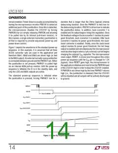
Manual Power-Up Via The PWRON Pin
duration, RESET will be released.
If the pushbutton interface is not required, the LTC3101
can be manually enabled by simply forcing the PWRON
pin high. When PWRON is forced high any channels that
are enabled via their independent enable pin will power
up in the standard sequence (buck converter 1, buck con-
verter 2 and then the buck-boost converter). An arbitrary
power-up sequence can be forced manually, by forcing all
enables (ENA1, ENA2, ENA3) low while bringing PWRON
high. Then, after waiting 10ꢀs for the logic to initialize,
theindividualconverterscanbemanuallyenabledviatheir
independentenablepinsinanyorderrequired.Forexample,
a simultaneous power-up is initiated by bringing PWRON
high while holding ENA1, ENA2 and ENA3 low. Then after
a 10μs or longer delay, ENA1, ENA2 and ENA3 can be
brought high simultaneously causing the two buck rails
and the buck-boost rail to begin rising simultaneously.
LDO OUTPUT
The LDO output generates a regulated 1.8V (nominal)
output voltage rail that is guaranteed to support a 50mA
load. The LDO output remains active whenever a valid
supply is present on either the USB2 or BAT2 inputs and
is unaffected by the pushbutton interface. Its always-on
status allows the LDO to power critical functions such as
a real time clock which must remain powered under all
conditions.
The LDO output is reverse blocking in shutdown (i.e.,
whenundervoltagelockoutthresholdisreached)allowing
its output to stay charged when both input supplies are
removedwithreverseleakageguaranteedtobeunder1μA.
This allows the LDO to be used to charge a supercapaci-
tor for memory retention purposes or powering standby
functions during times when both power sources are
removed. The LDO is specifically designed to be stable
with a small 4.7μF capacitor, but to also maintain stable
operationwitharbitrarilylargecapacitancesupercapacitors
without requiring a series isolation resistor.
Fault Conditions
On an overtemperature or input undervoltage fault condi-
tion, all DC/DC converters, the LDO, and the MAX output
are disabled and the C pin is driven low which results
RS
in the microprocessor reset output, RESET, being driven
low as well. In the standard application, this will cause
the microprocessor to release the PWRON pin, thereby
disablingtheLTC3101.Consequently,theLTC3101willnot
The LDO output is current-limit protected. On an
undervoltageorovertemperaturefault,theLDOisdisabled
until the fault condition clears.
3101f
15

 Linear [ Linear ]