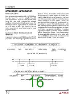
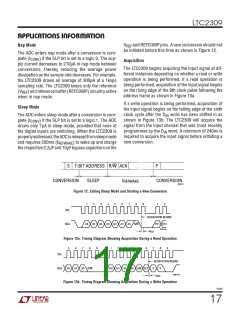
LTC2309
APPLICATIONS INFORMATION
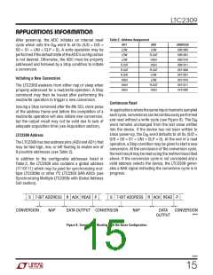
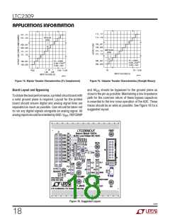
111...111
111...110
011...111
BIPOLAR
ZERO
011...110
100...001
100...000
011...111
011...110
000...001
000...000
111...111
111...110
UNIPOLAR
ZERO
FS = 4.096V
1LSB = FS/2
000...001
000...000
FS = 4.096V
1LSB = FS/2
100...001
100...000
12
12
1LSB = 1mV
1LSB = 1mV
–1 0V
1
0V
FS – 1LSB
–FS/2
FS/2 – 1LSB
LSB
LSB
INPUT VOLTAGE (V)
INPUT VOLTAGE (V)
2309 F15
2309 F14
Figure 14. Bipolar Transfer Characteristics (2’s Complement)
Figure 15. Unipolar Transfer Characteristics (Straight Binary)
Board Layout and Bypassing
and AV should be bypassed to the ground plane as
DD
close to the pin as possible. Maintaining a low impedance
path for the common return of these bypass capacitors
is essential to the low noise operation of the ADC. These
traces should be as wide as possible. See Figure 16 for a
suggested layout.
Toobtainthebestperformance,aprintedcircuitboardwith
a solid ground plane is required. Layout for the printed
board should ensure digital and analog signal lines are
separated as much as possible. Care should be taken not
to run any digital signals alongside an analog signal. All
analoginputsshouldbeshieldedbyGND.V ,REFCOMP
REF
Figure 16. Suggested Layout
2309f
18

 Linear [ Linear ]