LTC2309
APPLICATIONS INFORMATION
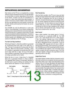
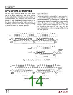
The data output stream is 16 bits long and is shifted
out on the falling edges of SCL (see Figure 8a). The
first bit is the MSB and the 12th bit is the LSB of the
conversion result. The remaining four bits are zero.
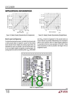
Figures 14 and 15 are the transfer characteristics for
the bipolar and unipolar modes. Data is output on the
SDA line in 2’s complement format for bipolar readings
or in straight binary for unipolar readings.
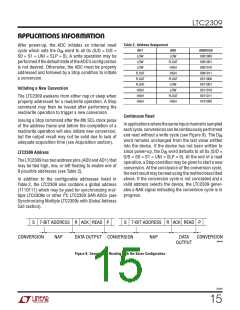
Input Data Format
When the LTC2309 is addressed for a write operation,
it acknowledges by pulling SDA low during the low
period before the 9th cycle and acts as a receiver. The
master/transmittercanthensend1bytetoprogramthe
device. The input byte consists of the 6-bit D word
IN
followed by two bits that are ignored by the ADC and
are considered don’t cares (X) (see Figure 8b). The
input bits are latched on the rising edge of SCL during
the write operation.
1
2
3
4
5
6
7
8
9
1
2
3
4
5
6
7
8
9
• • •
SCL
SDA
A6
A5
A4
A3
A2
A1
A0 R/W
B11 B10 B9
B8
B7
B6
B5 B4
• • •
START BY
MASTER
ACK BY
ADC
ACK BY
MASTER
MOST SIGNIFICANT DATA BYTE
READ 1 BYTE
ADDRESS FRAME
1
2
3
4
5
6
7
8
9
SCL
• • •
• • •
(CONTINUED)
CONVERSION
INITIATED
SDA
(CONTINUED)
STOP
BY MASTER
B3
B2
B1
B0
NAK BY
MASTER
LEAST SIGNIFICANT DATA BYTE
READ 1 BYTE
2309 F08a
Figure 8a. Timing Diagram for Reading from the LTC2309
1
2
3
4
5
6
7
8
9
1
2
3
4
5
6
7
8
9
SCL
SDA
CONVERSION
INITIATED
A6
A5
A4
A3
A2
A1
A0 R/W
S/D O/S S1
S0 UNI SLP
WORD
X
X
STOP BY
MASTER
START BY
MASTER
ACK BY
ADC
ACK BY
ADC
D
IN
2309 F08b
ADDRESS FRAME
WRITE 1 BYTE
Figure 8b. Timing Diagram for Writing to the LTC2309
2309f
14

 Linear [ Linear ]