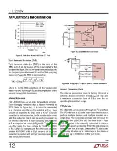
LTC2309
APPLICATIONS INFORMATION
Nap Mode
V
and REFCOMP pins. A new conversion should not
REF
be initiated before this time as shown in Figure 12.
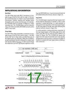
The ADC enters nap mode after a conversion is com-
plete (t
) if the SLP bit is set to a logic 0. The sup-
CONV
Acquisition
ply current decreases to 210ꢁA in nap mode between
conversions, thereby reducing the average power
dissipation as the sample rate decreases. For example,
the LTC2309 draws an average of 300μA at a 1ksps
sampling rate. The LTC2309 keeps only the reference
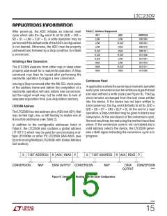
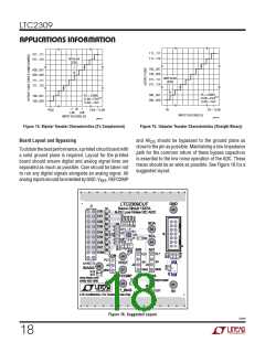
The LTC2309 begins acquiring the input signal at dif-
ferent instances depending on whether a read or write
operation is being performed. If a read operation is
being performed, acquisition of the input signal begins
on the rising edge of the 9th clock pulse following the
address frame as shown in Figure 13a.
(V )andreferencebuffer(REFCOMP)circuitryactive
REF
when in nap mode.
If a write operation is being performed, acquisition of
the input signal begins on the falling edge of the sixth
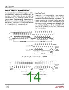
Sleep Mode
clock cycle after the D word has been shifted in as
The ADC enters sleep mode after a conversion is com-
IN
shown in Figure 13b. The LTC2309 will acquire the
plete (t
) if the SLP bit is set to a logic 1. The ADC
CONV
signal from the input channel that was most recently
draws only 7μA in sleep mode, provided that none of
the digital inputs are switching. When the LTC2309 is
properlyaddressed,theADCisreleasedfromsleepmode
programmed by the D word. A minimum of 240ns is
IN
required to acquire the input signal before initiating a
new conversion.
and requires 200ms (t
therespective2.2ꢁFand10ꢁFbypasscapacitorsonthe
) to wake up and charge
REFWAKE
S 7-BIT ADDRESS R/W ACK
P
CONVERSION
SLEEP
t
CONVERSION
REFWAKE
2309 F12
Figure 12. Exiting Sleep Mode and Starting a New Conversion
1
2
3
4
5
6
7
8
9
1
2
SCL
SDA
ACQUISITION BEGINS
A6
A5
A4
A3
A2
A1
A0 R/W
B11 B10
2309 F13a
t
ACQ
Figure 13a. Timing Diagram Showing Acquisition During a Read Operation
5
6
7
8
9
1
2
3
4
5
6
7
8
9
SCL
SDA
ACQUISITION BEGINS
A2
A1
A0 R/W
S/D O/S S1 S0 UNI SLP
X
X
2309 F13b
t
ACQ
Figure 13b. Timing Diagram Showing Acquisition During a Write Operation
2309f
17

 Linear [ Linear ]