LTC2309
APPLICATIONS INFORMATION
0
R1
8k
SNR = 73.4dB
V
REF
SINAD = 73.3dB
BANDGAP
–20
2.5V
THD = –88dB
REFERENCE
2.2μF
0.1μF
–40
REFCOMP
4.096V
10μF
–60
–80
REFERENCE
AMP
R2
–100
–120
–140
R3
GND
LTC2309
0
1
2
3
4
5
6
7
2309 F06a
FREQUENCY (kHz)
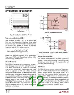
Figure 6a. LTC2309 Reference Circuit
2309 G03
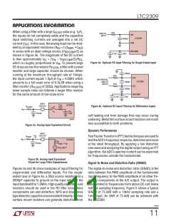
Figure 5. 1kHz Sine Wave 8192 Point FFT Plot
5V
0.1μF
Total Harmonic Distortion (THD)
V
IN
LT1790A-2.5
V
Total harmonic distortion (THD) is the ratio of the
RMS sum of all harmonics of the input signal to the
fundamentalitself.Theout-of-bandharmonicsaliasinto
the frequency band between DC and half the sampling
V
OUT
REF
2.2μF
0.1μF
LTC2309
REFCOMP
+
10μF
frequency(f
/2). THD is expressed as:
SMPL
GND
V 2 + V 2 + V42...+ V 2
2309 F06b
2
3
N
THD= 20log
Figure 6b. Using the LT®1790A-2.5 as an External Reference
V
1
where V is the RMS amplitude of the fundamental
1
Internal Conversion Clock
frequency and V through V are the amplitudes of the
2
N
The internal conversion clock is factory trimmed to
second through Nth harmonics.
achieve a typical conversion time (t
) of 1.3ꢁs and
CONV
Internal Reference
a maximum conversion time of 1.8ꢁs over the full
operating temperature range.
The LTC2309 has an on-chip, temperature compen-
sated bandgap reference that is factory trimmed to
2.5V (Refer to Figure 6a). It is internally connected
2
I C Interface
2
The LTC2309 communicates through an I C interface.
to a reference amplifier and is available at V . V
REF REF
2
The I C interface is a 2-wire open-drain interface sup-
should be bypassed to GND with a 2.2ꢁF tantalum
capacitor to minimize noise. An 8k resistor is in series
with the output so that it can be easily overdriven by
an external reference if more accuracy and/or lower
drift are required as shown in Figure 6b. The reference
porting multiple devices and multiple masters on a
single bus. The connected devices can only pull the
serial data line (SDA) low and can never drive it high.
SDA is required to be externally connected to the sup-
ply through a pull-up resistor. When the data line is not
amplifier gains the V
voltage by 1.638 to 4.096V
REF
2
being driven low, it is high. Data on the I C bus can be
transferred at rates up to 100kbits/s in the standard
mode and up to 400kbits/s in the fast mode.
at REFCOMP. To compensate the reference amplifier,
bypass REFCOMP with a 10ꢁF ceramic or tantalum
capacitor in parallel with a 0.1ꢁF ceramic capacitor for
best noise performance.
2309f
12

 Linear [ Linear ]