LT8705
APPLICATIONS INFORMATION
dissipated while the switch is turning “on” or “off”. As the
switch turns “on” and “off” a combination of high current
and high voltage causes high power dissipation in the
MOSFET.Althoughtheswitchingtimesareshort,theaver-
age power dissipation can still be significant and is often
the dominant source of power in the MOSFET. Depending
on the application, the maximum power dissipation in
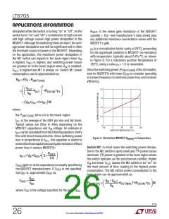
R
is the series gate resistance of the MOSFET
GATE
(usually < 1Ω—see manufacturer’s data sheet) plus
any additional resistance connected in series with the
MOSFET’s gate.
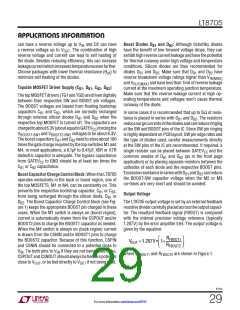
ρ is a normalization factor (unity at 25°C) accounting
τ
for the significant variation in MOSFET on-resistance
with temperature, typically about 0.4%/°C, as shown
in Figure 9. For a maximum junction temperature of
the M1 switch can happen in the buck region when V
IN
is highest, V
is highest, and switching power losses
OUT
125°C, using a value ρ = 1.5 is reasonable.
τ
are greatest or in the boost region when V is smallest,
IN
Since the switching power (P
look for MOSFETs with lower C
at a lower frequency to minimize power loss and increase
efficiency.
) often dominates,
V
OUT
is highest and M1 is always on. Switch M1 power
SWITCHING
or consider operating
consumption can be approximated as:
RSS
2
PM1 = P + P
I R
SWITCHING
2
VOUT
2.0
1.5
1.0
0.5
0
≅
•IOUT •RDS(ON) •ρτ
V
IN
+ V •I
•f•tRF1 W
(
)
IN
OUT
where:
the P
term is 0 in the boost region
SWITCHING
t
is the average of the SW1 pin rise and fall times.
RF1
Typical values are 20ns to 40ns depending on the
MOSFET capacitance and V voltage. An estimate of
50
100
–50
150
0
IN
JUNCTION TEMPERATURE (°C)
t
canbecalculatedfromthefollowingequation.Verify
RF1
8705 F09
this with direct measurements. Since switching power
Figure 9. Normalized MOSFET RDS(ON) vs Temperature
loss is proportional to t , this equation is useful to
RF1
understandhowcapacitanceandgateresistanceeffects
Switch M2: In most cases the switching power dissipa-
power loss in various MOSFETs:
2
tion in the M2 switch is quite small and I R power losses
R
GATE
• 2+
2
dominate. I R power is greatest in the buck region where
tRF1 ≅ V •C
IN
RSS
0.8
the switch operates as the synchronous rectifier. Higher
V and lower V
causes the M2 switch to be “on” for
IN
OUT
C
(gate-to-draincapacitance)isusuallyspecifiedby
RSS
the most amount of time, leading to the highest power
consumption. The M2 switch power consumption in the
buck region can be approximated as:
the MOSFET manufacturers. If C
is not specified,
RSS
but Q is, approximate C
as:
GD
RSS
QGD
VDS
CRSS
=
V – V
IN
OUT
P
≅
•IOUT(MAX)2 •RDS(ON) •ρτ W
(M2,BUCK)
V
IN
where V is the voltage specified for the given Q .
DS
GD
8705p
26
For more information www.linear.com/8705

 Linear [ Linear ]