LT8705
OPERATION
is turned on first. Inductor current is sensed by amplifier
A5 while switch M2 is on. A slope compensation ramp is
addedtothesensedvoltagewhichisthencomparedbyA8
charging up to 2.5V and be held there in the case of a fault
eventthatpersists. Afterthefaultconditionhadendedand
SS is greater than 1.6V, SS will then slowly discharge to
50mV (post fault delay state). This timeout period relieves
the part and other downstream power components from
electrical and thermal stress for a minimum amount of
time as set by the voltage ramp rate on the SS pin. After
SS has discharged to < 50mV, the LT8705 will enter the
soft-start state and restart switching activity.
to a reference that is proportional to V . After the sensed
C
inductor current falls below the reference, switch M2 is
turned off and switch M1 is turned on for the remainder
of the cycle. Switches M1 and M2 will alternate, behaving
like a typical synchronous buck regulator.
CLOCK
Power Switch Control
SWITCH M1
SWITCH M2
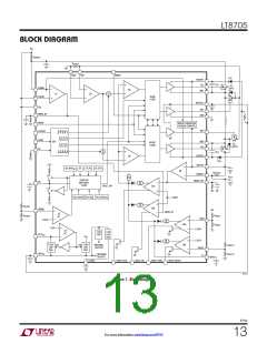
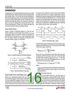
Figure 3 shows a simplified diagram of how the four
power switches are connected to the inductor, V , V
IN OUT
OFF
SWITCH M3
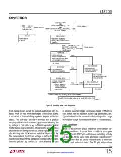
and ground. Figure 4 shows the regions of operation for
ON
SWITCH M4
the LT8705 as a function of V -V or switch duty cycle
OUT IN
I
L
DC. The power switches are properly controlled so the
8705 F05
transfer between modes is continuous.
Figure 5. Buck Region (VIN >> VOUT
)
V
IN
V
OUT
The part will continue operating in the buck region over a
rangeofswitchM2dutycycles.ThedutycycleofswitchM2
in the buck region is given by:
TG1
BG1
M1
SW1
M4
TG2
BG2
L
SW2
M2
M3
VOUT
DC(M2,BUCK) = 1–
•100%
V
R
SENSE
IN
8705 F03
As V and V
get closer to each other, the duty cycle
IN
OUT
Figure 3. Simplified Diagram of the Output Switches
decreases until the minimum duty cycle of the converter
in buck mode reaches DC . If the duty
SWITCH
(ABSMIN,M2,BUCK)
M3 DC
MAX
cycle becomes lower than DC
will move to the buck-boost region.
the part
(ABSMIN,M2,BUCK)
M1 ON, M2 OFF
PWM M3, M4 SWITCHES
BOOST REGION
SWITCH
M3 DC
MIN
DC ≅ t
• f • 100%
ON(M2,MIN)
0
BUCK/BOOST REGION 4-SWITCH PWM
(ABSMIN,M2,BUCK)
SWITCH
M2 DC
MIN
where:
M4 ON, M3 OFF
BUCK REGION
PWM M1, M2 SWITCHES
t
istheminimumon-timeforthesynchronous
ON(M2,MIN)
SWITCH
8705 F04
M2 DC
MAX
switch in buck operation (260ns typical, see Electrical
Characteristics).
Figure 4. Operating Regions vs VOUT-VIN
f is the switching frequency
Power Switch Control: Buck Region (V >> V
)
OUT
IN
When V is much higher than V
the duty cycle of
IN
OUT
switch M2 will increase, causing the M2 switch off-time
to decrease. The M2 switch off-time should be kept above
245ns (typical, see Electrical Characteristics) to maintain
steady-state operation, avoid duty cycle jitter, increased
When V is significantly higher than V , the part will
IN
OUT
run in the buck region. In this region switch M3 is always
off. Also, switch M4 is always on unless reverse current is
detected while in Burst Mode operation or discontinuous
mode. At the start of every cycle, synchronous switch M2
output ripple and reduction in maximum output current.
8705p
16
For more information www.linear.com/8705

 Linear [ Linear ]