LT8705
OPERATION
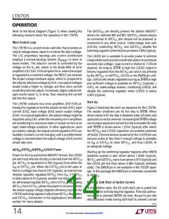
T
< 160°C
JUNCTION
AND
SHDN > 1.234V AND V > 2.5V
IN
SHDN < 1.184V OR
< 2.5V OR
TYPICAL VALUES
AND
TYPICAL VALUES
V
IN
JUNCTION
(SWEN* < 1.184V OR (INTV AND GATEV < 4.65V)
CC
CC
T
> 165°C
OR LDO33 < 3.04V)
CHIP OFF
SWITCHER OFF
• SWITCHER OFF
• LDOs OFF
• SWITCHER DISABLED
• INTV AND LDO33 OUTPUTS
CC
ENABLED
SHDN > 1.234V AND V > 2.5V
IN
AND SWEN* > 1.206V AND
TYPICAL VALUES
(INTV AND GATEV > 4.81V) AND
CC
CC
LDO33 > 3.075V
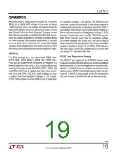
INITIALIZE
• SS PULLED LOW
FAULT
• FORCE DISCONTINOUS
MODE UNLESS Burst Mode
OPERATION SELECTED
SS < 50mV
FAULT DETECTED
SOFT-START
FAULT
FAULT
• SS CHARGES UP
• SWITCHER DISABLED
• CLKOUT DISABLED
• SS CHARGES UP
• SWITCHER ENABLED
SS > 1.6V AND
NO FAULT CONDITIONS
STILL DETECTED
NORMAL MODE
• NORMAL OPERATION
• WHEN SS > 1.6V ...
• CLKOUT ENABLED
• ENABLE FORCED
CONTINUOUS MODE
IF SELECTED
POST FAULT DELAY
FAULT
• SS SLOWLY DISCHARGES
SS < 50mV
*SWEN IS CONNECTED TO INTV IN THE TSSOP PACKAGE
CC
FAULT = OVERVOLTAGE (IMON_IN OR IMON_OUT > 1.61V TYP)
8705 F02
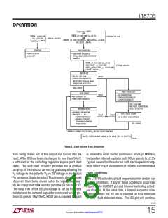
Figure 2. Start-Up and Fault Sequence
from being drawn out of the output and forced into the
input. After SS has been discharged to less than 50mV,
a soft-start of the switching regulator begins (soft-start
state). The soft-start circuitry provides for a gradual
ramp-up of the inductor current by gradually allowing the
is allowed to enter forced continuous mode (if MODE is
low)andaninternalregulatorpullsSSupquicklyto≅2.5V.
Typical values for the external soft-start capacitor range
from 100nF to 1μF. A minimum of 100nF is recommended.
Fault Conditions
V voltage to rise (refer to V vs SS Voltage in the Typical
C
C
PerformanceCharacteristics).Thispreventsabruptsurges
of current from being drawn out of the input power sup-
ply. An integrated 100k resistor pulls the SS pin to ≅2.5V.
The ramp rate of the SS pin voltage is set by this 100k
resistor and the external capacitor connected to this pin.
Once SS gets to 1.6V, the CLKOUT pin is enabled, the part
The LT8705 activates a fault sequence under certain op-
erating conditions. If any of these conditions occur (see
Figure 2) the CLKOUT pin and internal switching activity
are disabled. At the same time, a timeout sequence com-
mences where the SS pin is charged up to a minimum
of 1.6V (fault detected state). The SS pin will continue
8705p
15
For more information www.linear.com/8705

 Linear [ Linear ]