LT8705
OPERATION
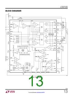
Refer to the Block Diagram (Figure 1) when reading the
following sections about the operation of the LT8705.
The GATEV pin directly powers the bottom MOSFET
CC
drivers for switches M2 and M3. GATEV should always
CC
be connected to INTV and should not be powered or
CC
Main Control Loop
connected to any other source. Undervoltage lock outs
(UVLOs) monitoring INTV and GATEV disable the
CC
CC
The LT8705 is a current mode controller that provides an
output voltage above, equal to or below the input voltage.
The LTC proprietary topology and control architecture
switchingregulatorwhenthepinsarebelow4.65V(typical).
The LDO33 pin is available to provide power to external
componentssuchasamicrocontrollerand/ortoprovidean
accurate bias voltage. Load current is limited to 17.25mA
(typical). As long as SHDN is high the LDO33 output is
employs a current-sensing resistor (R
) in buck or
SENSE
boost modes. The inductor current is controlled by the
voltage on the V pin, which is the diode-AND of error
C
amplifiersEA1-EA4.Inthesimplestform,wheretheoutput
is regulated to a constant voltage, the FBOUT pin receives
the output voltage feedback signal, which is compared to
theinternalreferencevoltagebyEA4.Lowoutputvoltages
linearly regulated from the INTV pin and is not affected
CC
by the INTV or GATEV UVLOs or the SWEN pin volt-
CC
CC
age. LDO33 will remain regulated as long as SHDN is high
and sufficient voltage is available on INTV (typically >
CC
would create a higher V voltage, and thus more current
4.0V). An undervoltage lockout, monitoring LDO33, will
disable the switching regulator when LDO33 is below
3.04V (typical).
C
wouldflowintotheoutput. Conversely, higheroutputvolt-
ages would cause V to drop, thus reducing the current
C
fed into the output.
Start-Up
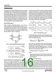
The LT8705 contains four error amplifiers (EA1-EA4) al-
lowing it to regulate or limit the output current (EA1), input
current (EA2), input voltage (EA3) and/or output voltage
(EA4). In a typical application, the output voltage might be
regulated using EA4, while the remaining error amplifiers
are monitoring for excessive input or output current or an
input undervoltage condition. In other applications, such
asabatterycharger,theoutputcurrentregulator(EA1)can
facilitate constant current charging until a predetermined
voltage is reached where the output voltage (EA4) control
would take over.
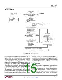
Figure 2 illustrates the start-up sequence for the LT8705.
The master shutdown pin for the chip is SHDN. When
driven below 0.4V the chip is disabled (chip off state) and
quiescentcurrentisminimal.IncreasingtheSHDNvoltage
can increase quiescent current but will not enable the chip
until SHDN is driven above 1.234V (typical) after which
the INTV and LDO33 regulators are enabled (switcher
CC
off state). External devices powered by the LDO33 pin can
become active at this time if enough voltage is available
on V or EXTV to raise INTV , and thus LDO33, to
IN
CC
CC
an adequate voltage.
INTV /EXTV /GATEV /LDO33 Power
CC
CC
CC
Starting up the switching regulator happens after SWEN
(switcher enable) is also driven above 1.206V (typical),
INTV and GATEV haverisenabove4.81V(typical)and
Power for thetopand bottomMOSFET drivers, the LDO33
pin and most internal circuitry is derived from the INTV
CC
CC
CC
pin. INTV is regulated to 6.35V (typical) from either the
the LDO33 pin has risen above 3.08V (typical) (initialize
state). The SWEN pin is not available in the TSSOP pack-
age. In this package the SWEN pin is internally connected
CC
V or EXTV pin. When the EXTV pin is left open or
IN
CC
CC
tied to a voltage less than 6.22V (typical), an internal low
dropout regulator regulates INTV from V . If EXTV
CC
to INTV .
CC
IN
CC
is taken above 6.4V (typical), another low dropout regula-
tor will instead regulate INTV from EXTV . Regulating
Start-Up: Soft-Start of Switch Current
CC
CC
INTV from EXTV allows the power to be derived from
CC
CC
In the initialize state, the SS (soft-start) pin is pulled low
toprepareforsoftstartingtheregulator. Ifforcedcontinu-
ous mode is selected (MODE pin low), the part is put into
discontinuous mode during soft-start to prevent current
8705p
the lowest supply voltage (highest efficiency) such as the
LT8705switchingregulatoroutput(seeINTV Regulators
CC
and EXTV Connection in the Applications Information
CC
section for more details).
14
For more information www.linear.com/8705

 Linear [ Linear ]