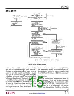
LT8705
(QFN/TSSOP)
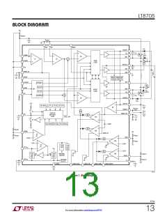
PIN FUNCTIONS
SHDN (Pin 1/Pin 4): Shutdown Pin. Tie high to enable
device.Groundtoshutdownandreducequiescentcurrent
to a minimum. Do not float this pin.
RT(Pin12/Pin15):TimingResistorPin.Adjuststheswitch-
ing frequency. Place a resistor from this pin to ground to
set the free-running frequency. Do not float this pin.
CSN (Pin 2/Pin 5): The (–) Input to the Inductor Current
BG1, BG2 (Pins 14, 16/Pins 17, 19): Bottom Gate Drive.
Sense and Reverse-Current Detect Amplifier.
Drives the gates of the bottom N-channel MOSFETs be-
tween ground and GATEV .
CC
CSP (Pin 3/Pin 6): The (+) Input to the Inductor Current
Sense and Reverse-Current Detect Amplifier. The V pin
GATEV (Pin 15/Pin 18): Power Supply for Gate Drivers.
CC
C
voltage and built-in offsets between CSP and CSN pins, in
Must be connected to the INTV pin. Do not power from
CC
conjunction with the R
trip threshold.
resistor value, set the current
any other supply. Locally bypass to GND.
SENSE
BOOST1, BOOST2 (Pins 23, 17/Pins 28, 20): Boosted
Floating Driver Supply. The (+) terminal of the bootstrap
capacitor connects here. The BOOST1 pin swings from a
LDO33 (Pin 4/Pin7): 3.3V Regulator Output. Bypass this
pin to ground with a minimum 0.1μF ceramic capacitor.
diode voltage below GATEV up to V + GATEV . The
CC
IN
CC
FBIN (Pin 5/Pin 8): Input Feedback Pin. This pin is con-
nected to the input error amplifier input.
BOOST2 pin swings from a diode voltage below GATEV
CC
up to V
+ GATEV
OUT
CC
FBOUT (Pin 6/Pin 9): Output Feedback Pin. This pin
connects the error amplifier input to an external resistor
divider from the output.
TG1,TG2(Pins22,18/Pins26,21):TopGateDrive.Drives
the top N-channel MOSFETs with voltage swings equal
to GATEV superimposed on the switch node voltages.
CC
IMON_OUT(Pin7/Pin10):OutputCurrentMonitorPin.The
currentoutofthispinisproportionaltotheoutputcurrent.
See the Operation and Applications Information sections.
SW1, SW2 (Pins 21, 19/Pins 24, 22): Switch Nodes. The
(–) terminals of the bootstrap capacitors connect here.
SRVO_FBIN (Pin 25 QFN Only): Open-Drain Logic Out-
put. This pin is pulled to ground when the input voltage
feedback loop is active.
V (Pin 8/Pin 11): Error Amplifier Output Pin. Tie external
C
compensation network to this pin.
SS (Pin 9/Pin 12): Soft-Start Pin. Place at least 100nF of
capacitance here. Upon start-up, this pin will be charged
by an internal resistor to 2.5V.
SRVO_IIN (Pin 26 QFN Only): Open-Drain Logic Output.
The pin is pulled to ground when the input current loop
is active.
CLKOUT (Pin 10/Pin 13): Clock Output Pin. Use this pin to
synchronize one or more compatible switching regulator
ICs to the LT8705. CLKOUT toggles at the same frequency
as the internal oscillator or as the SYNC pin, but is ap-
proximately 180° out of phase. CLKOUT may also be used
as a temperature monitor since the CLKOUT duty cycle
varies linearly with the part’s junction temperature. The
CLKOUT pin can drive capacitive loads up to 200pF.
SRVO_IOUT (Pin 27 QFN Only): Open-Drain Logic Out-
put. The pin is pulled to ground when the output current
feedback loop is active.
SRVO_FBOUT (Pin 28 QFN Only): Open-Drain Logic Out-
put. This pin is pulled to ground when the output voltage
feedback loop is active.
EXTV (Pin29/Pin30):ExternalV Input.WhenEXTV
CC
CC
CC
SYNC (Pin 11/Pin 14): To synchronize the switching fre-
quency to an outside clock, simply drive this pin with a
clock. The high voltage level of the clock needs to exceed
1.3V, and the low level should be less than 0.5V. Drive this
pin to less than 0.5V to revert to the internal free-running
clock. See the Applications Information section for more
information.
exceeds 6.4V (typical), INTV will be powered from this
CC
pin. When EXTV is lower than 6.22V (typical), INTV
CC
CC
will be powered from V .
IN
CSNOUT (Pin 30/Pin 32): The (–) Input to the Output Cur-
rent Monitor Amplifier. Connect this pin to V
when not
OUT
in use. See Applications Information section for proper
use of this pin.
8705p
11
For more information www.linear.com/8705

 Linear [ Linear ]