LT3580
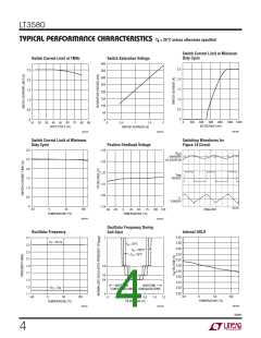
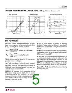
TYPICAL PERFORMANCE CHARACTERISTICS TA = 25°C unless otherwise specified
SHDN Pin Current
SHDN Pin Current
Active/Lockout Threshold
1.40
1.38
1.36
1.34
1.32
1.30
1.28
1.26
1.24
1.22
1.20
30
25
300
250
200
150
–50°C
20°C
100°C
20
15
SHDN RISING
SHDN FALLING
10
5
100
50
0
–50°C
20°C
100°C
0
–50
0
50
100
0
0.5
1
1.5
2
20
SHDN VOLTAGE (V)
30
0
5
10
15
25
TEMPERATURE (°C)
SHDN VOLTAGE (V)
3580 G12
3580 G10
3580 G11
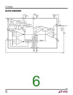
PIN FUNCTIONS
FB (Pin 1): Positive and Negative Feedback Pin. For a
RT (Pin 6): Timing Resistor Pin. Adjusts the switching
frequency. Place a resistor from this pin to ground to set
the frequency to a fixed free running level. Do not float
this pin.
boost or inverting converter, tie a resistor from the FB pin
to V
according to the following equations:
OUT
V
ꢀ1.215
(
)
OUT
RFB =
RFB =
; Boost or SEPIC Converter
SS(Pin7):Soft-StartPin.Placeasoft-startcapacitorhere.
Upon start-up, the SS pin will be charged by a (nominally)
275k resistor to about 2.2V.
83.3•10ꢀ6
V
83.3•10ꢀ6
+ 5mV
(
)
OUT
; Inverting Converter
SYNC (Pin 8): To synchronize the switching frequency to
an outside clock, simply drive this pin with a clock. The
high voltage level of the clock needs to exceed 1.3V, and
the low level should be less 0.4V. Drive this pin to less than
0.4V to revert to the internal free running clock. See the
Applications Information section for more information.
VC (Pin 2): Error Amplifier Output Pin. Tie external com-
pensation network to this pin.
V (Pin 3): Input Supply Pin. Must be locally bypassed.
IN
SW (Pin 4): Switch Pin. This is the collector of the internal
NPN Power switch. Minimize the metal trace area con-
nected to this pin to minimize EMI.
Exposed Pad (Pin 9): Ground. Must be soldered directly
to local ground plane.
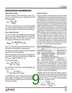
SHDN (Pin 5): Shutdown Pin. In conjunction with the
UVLO (undervoltage lockout) circuit, this pin is used
to enable/disable the chip and restart the soft-start
sequence. Drive below 1.24V to disable the chip. Drive
above 1.38V to activate chip and restart the soft-start
sequence. Do not float this pin.
3580fc
5

 Linear [ Linear ]