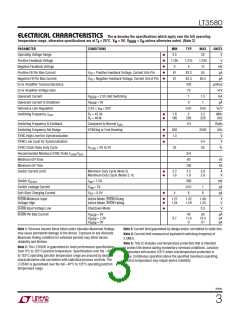
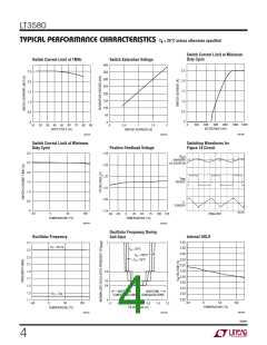
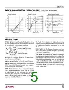
LT3580
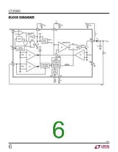
OPERATION
The LT3580 uses a constant-frequency, current mode
control scheme to provide excellent line and load regula-
tion. Refer to the Block Diagram which shows the LT3580
in a boost configuration. At the start of each oscillator
cycle, the SR latch (SR1) is set, which turns on the power
switch, Q1. The switch current flows through the internal
current sense resistor generating a voltage proportional
to the switch current. This voltage (amplified by A4) is
added to a stabilizing ramp and the resulting sum is fed
into the positive terminal of the PWM comparator A3.
When this voltage exceeds the level at the negative input
of A3, the SR latch is reset, turning off the power switch.
The level at the negative input of A3 (VC pin) is set by the
error amplifier A1 (or A2) and is simply an amplified ver-
sion of the difference between the feedback voltage (FB
pin) and the reference voltage (1.215V or 5mV depending
on the configuration). In this manner, the error amplifier
sets the correct peak current level to keep the output in
regulation.
configuration, the FB pin is pulled down to 5mV by the
R
resistor connected from V
to FB. Comparator
FB
OUT
A1 becomes inactive and comparator A2 performs the
noninverting amplification from FB to VC.
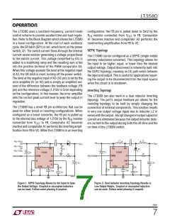
SEPIC Topology
The LT3580 can be configured as a SEPIC (single-ended
primary inductance converter). This topology allows for
the input to be higher, equal, or lower then the desired
output voltage. Output disconnect is inherently built into
the SEPIC topology, meaning no DC path exists between
the input and output. This is useful for applications requir-
ing the output to be disconnected from the input source
when the circuit is in shutdown.
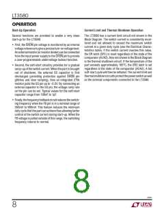
Inverting Topology
The LT3580 can also work in a dual inductor inverting
topology. The part’s unique feedback pin allows for the
inverting topology to be built by simply changing the
connection of external components. This solution results
in very low output voltage ripple due to inductor L2 in
serieswiththeoutput.Abruptchangesinoutputcapacitor
current are eliminated because the output inductor deliv-
ers current to the output during both the off-time and the
on-time of the LT3580 switch.
The LT3580 has a novel FB pin architecture that can be
used for either boost or inverting configurations. When
configured as a boost converter, the FB pin is pulled up
to the internal bias voltage of 1.215V by the R resistor
FB
connected from V
to FB. Comparator A2 becomes
OUT
inactive and comparator A1 performs the inverting ampli-
fication from FB to VC. When the LT3580 is in an inverting
C2
C2
L1
L2
L1
D1
R1
V
V
V
> V
= V
< V
•
•
IN
OUT
OR
OUT
OR
•
V
IN
V
V
OUT
OUT
•
L2
IN
IN
V
SW
V
SW
IN
IN
D1
+
+
OUT
C1
LT3580
C1
LT3580
R1
SHDN
FB
SHUTDOWN
SHDN
FB
SHUTDOWN
RT
GND
VC
+
RT
GND
VC
C3
C3
+
SYNC
SS
SYNC
SS
RC
CC
RC
CC
RT
C
RT
C
SS
SS
3580 F02
3580 F01
Figure 1. SEPIC Topology Allows for the Input to Span
the Output Voltage. Coupled or uncoupled inductors
can be used. Follow noted phasing if coupled.
Figure 2. Dual Inductor Inverting Topology Results in
Low Output Ripple. Coupled or uncoupled inductors
can be used. Follow noted phasing if coupled.
3580fc
7

 Linear [ Linear ]