LT1576/LT1576-5
U
W U U
APPLICATIONS INFORMATION
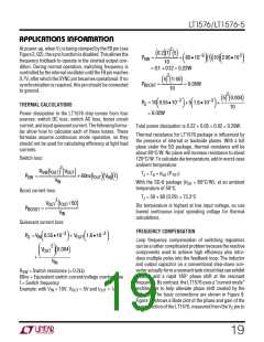
The output of the regulator contains both the desired low
frequency transient information and a reasonable amount
of high frequency (200kHz) ripple. The ripple makes it
difficult to observe the small transient, so a two-pole,
100kHz filter has been added. This filter is not particularly
critical; even if it attenuated the transient signal slightly,
this wouldn’t matter because amplitude is not critical.
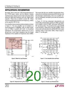
probably not be a problem in production. Note that fre-
quency of the light load ringing may vary with component
tolerance but phase margin generally hangs in there.
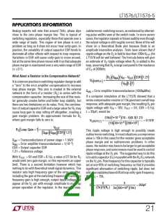
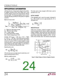
POSITIVE-TO-NEGATIVE CONVERTER
The circuit in Figure 15 is a classic positive-to-negative
topology using a grounded inductor. It differs from the
standard approach in the way the IC chip derives its
feedback signal, however, because the LT1576 accepts
onlypositivefeedbacksignals,thegroundpinmustbetied
to the regulated negative output. A resistor divider to
ground or, in this case, the sense pin, then provides the
proper feedback voltage for the chip.
After verifying that the setup is working correctly, I start
varying load current and input voltage to see if I can find
any combination that makes the transient response look
suspiciously “ringy.” This procedure may lead to an ad-
justment for best loop stability or faster loop transient
response. Nearly always you will find that loop response
looks better if you add in several kΩ for RC. Do this only
if necessary, because as explained before, RC above 1k
may require the addition of CF to control VC pin ripple.
If everything looks OK, I use a heat gun and cold spray on
the circuit (especially the output capacitor) to bring out
any temperature-dependent characteristics.
D1
1N4148
C2
0.33µF
L1*
15µH
INPUT
5.5V TO
20V
BOOST
LT576
V
V
IN
SW
R1
15.8k
Keep in mind that this procedure does not take initial
component tolerance into account. You should see fairly
cleanresponseunderallloadandlineconditionstoensure
that component variations will not cause problems. One
note here: according to Murphy, the component most
likely to be changed in production is the output capacitor,
because that is the component most likely to have manu-
facturer variations (in ESR) large enough to cause prob-
lems. It would be a wise move to lock down the sources of
the output capacitor in production.
FB
+
C3
10µF TO
50µF
GND
V
C
C1
+
R2
100µF
10V TANT
×2
4.99k
C
C
D2
1N5818
R
C
OUTPUT**
–5V, 0.5A
* INCREASE L1 TO 30µH OR 60µH FOR HIGHER CURRENT APPLICATIONS.
SEE APPLICATIONS INFORMATION
** MAXIMUM LOAD CURRENT DEPENDS ON MINIMUM INPUT VOLTAGE
AND INDUCTOR SIZE. SEE APPLICATIONS INFORMATION
1576 F15
Figure 15. Positive-to-Negative Converter
A possible exception to the “clean response” rule is at very
light loads, as evidenced in Figure 14 with ILOAD = 50mA.
Switching regulators tend to have dramatic shifts in loop
response at very light loads, mostly because the inductor
currentbecomesdiscontinuous.Onecommonresultisvery
slow but stable characteristics. A second possibility is low
phase margin, as evidenced by ringing at the output with
transients. The good news is that the low phase margin at
lightloadsisnotparticularlysensitivetocomponentvaria-
tion, so if it looks reasonable under a transient test, it will
Inverting regulators differ from buck regulators in the
basicswitchingnetwork. Currentisdeliveredtotheoutput
as square waves with a peak-to-peak amplitude much
greater than load current. This means that maximum load
current will be significantly less than the LT1576’s 1.5A
maximumswitchcurrent, evenwithlargeinductorvalues.
The buck converter in comparison, delivers current to the
output as a triangular wave superimposed on a DC level
equal to load current, and load current can approach 1.5A
23

 Linear [ Linear ]